W25N01GVXX Part Drivers Documentation 
This page presents an overview of the W25N01GVXX Part Drivers.
A detailed API documentation is also available here: W25N01GVXX Part Drivers API Documentation.
Introduction 
The W25N01GVXX part driver provides APIs to drive the W25N01GVXX NAND Flash. The implementation uses the HAL.
The W25N01GVXX is 3.3V (2.7V to 3.6V volts) 1G-bit Serial SLC NAND SPI flash memory organized into 65,536 programmable pages of 2,048-bytes each. The entire page can be programmed at one time using an internal 2,048-Byte buffer. Pages can be erased in groups of 64 (128KB block erase). To provide better NAND flash memory manageability, this memory also features user configurable internal ECC and bad block management.
The W25N01GVXX provides a continuous Read Mode that allows for efficient access to the entire memory array with a single Read command.
It is rated for more than 100,000 erase/program cycles with more than 10 years data retention.
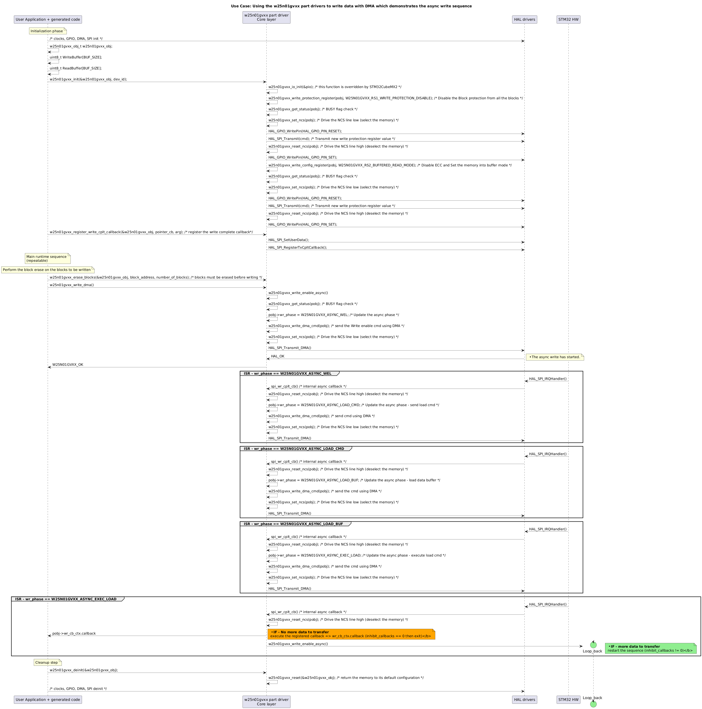
The W25N01GVXX part driver provides full asynchronous write functionality, including multi-page writes management through the use of an internal asynchronous state machine.
To use this feature, both
USE_HAL_SPI_REGISTER_CALLBACKS
and
USE_HAL_SPI_USER_DATA
must be enabled, and the write complete callback may be registered with the
w25n01gvxx_register_write_cplt_callback()
API.
The state machine starts with the call to
w25n01gvxx_write_dma()
and stops when all data has been transmitted. At that point, the previously registered callback function will be called.
The function
w25n01gvxx_get_async_write_phase()
allows to monitor the current transfer phase.
The driver for the W25N01GVXX comes as an OpenCMSIS pack. The following section describes its usage and the structure of the pack, providing a comprehensive guide to leveraging this high-performance flash memory device in your applications.
Principles 
The driver implements all functions in a single component. It uses the HAL SPI.
It abstracts SPI commands through easy-to-use straightforward APIs.
Programming model 
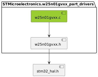
Folder structure 
The driver’s folder structure is as follows:
w25n01gvxx
  |- w25n01gvxx.c
  |- w25n01gvxx.h
The files w25n01gvxx.c, w25n01gvxx.h constitute the core of the part driver.
Usage and initialization 
The main data structure for this driver is the w25n01gvxx_obj_t object structure, which contains all the internal state needed by the driver. The user application never needs to access that structure’s fields directly. However, unlike with HAL drivers, the user application has full ownership of the data structures used by part driver. It is its duty to ensure timely allocation and de-allocation.
The driver has its own interface object structure, w25n01gvxx_io_t to store its own specific state and link to the underlying (HAL) driver being used.
At initialization, the user application must separately initialize the resources used by the part drivers, including the SPI peripheral as the part interface, the system peripherals, and the DMA peripheral (if using the part driver in DMA mode). Optionally, it can rely on STM32CubeMX2-generated code for the initialization of those HAL resources.
The part driver does not enforce the requirements on the resources, but the user application must respect them to ensure proper functionality. After the user application properly initializes all the required resources (HAL instances), it can call the part driver initialization and provide those resources.
When the user application initializes the part driver with the
w25n01gvxx_init()
function, it disables all block protection (power-on default: enabled), configures the read_mode as
W25N01GVXX_BUFFER_MODE
(power-on default:
W25N01GVXX_CONTINUOUS_MODE), and disables ECC. The user application can reconfigure these settings with the
w25n01gvxx_write_protection_register()
,
w25n01gvxx_set_read_mode()
, and
w25n01gvxx_enable_ecc()
functions.
Key part driver’s features: 
Read/Write operations in polling mode 
The W25N01GVXX part driver provides read and write APIs, which abstract the various commands involved in the process. This includes sending the write command, filling the buffer with the write data, and executing the load onto the physical memory.
w25n01gvxx_write() 
The W25N01GVXX features a 2048-byte data buffer (equivalent to one page size), which enables data caching but also limits the amount of data that can be written in a single transfer to this size. The w25n01gvxx_write() API overcomes this limitation by dynamically writing multiple pages based on the size provided.
w25n01gvxx_read() 
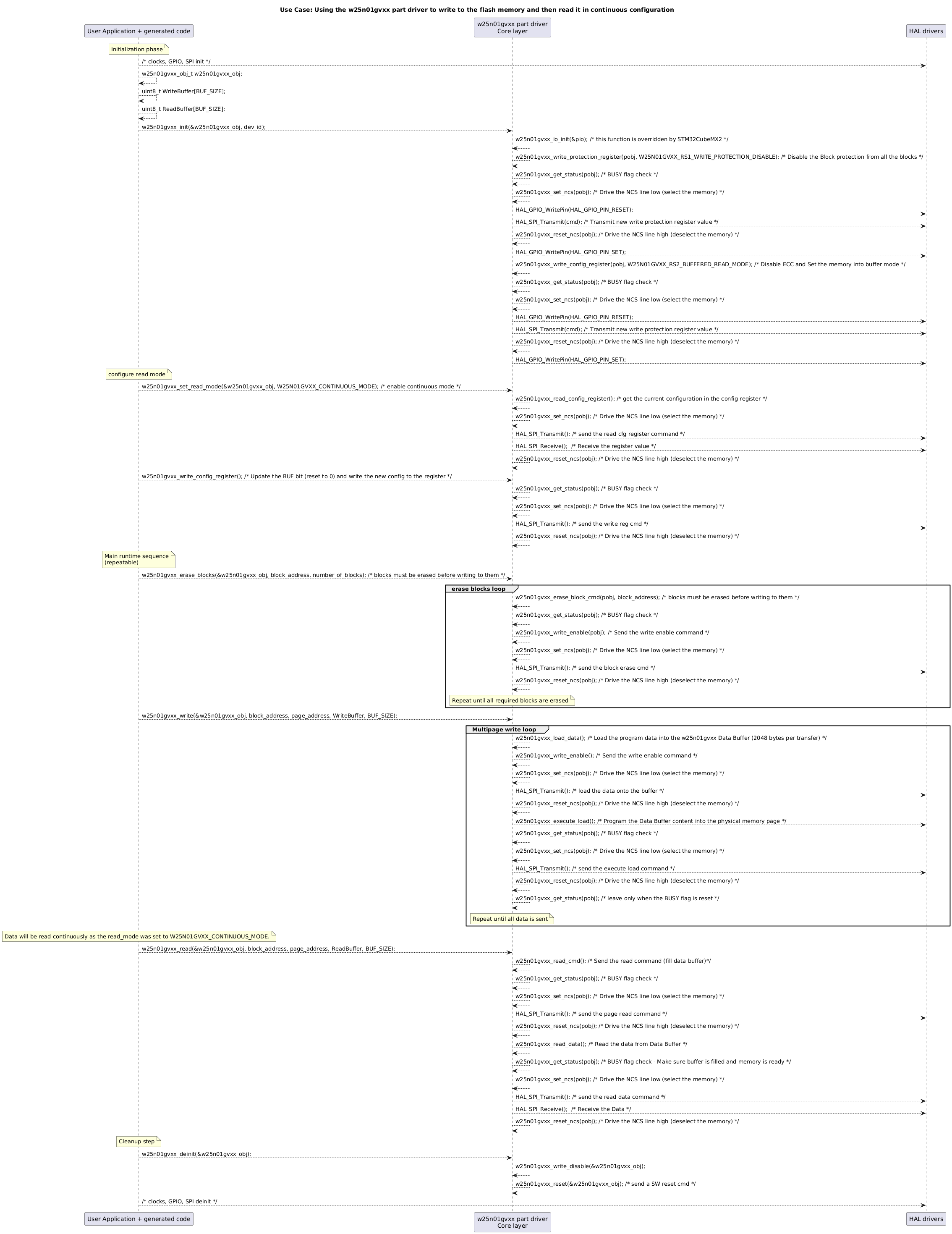
The W25N01GVXX supports two read modes: W25N01GVXX_BUFFER_MODE (default) and W25N01GVXX_CONTINUOUS_MODE.
When reading more than one page (2048 bytes) in a single transfer CONTINUOUS_MODE must be used/configured using the w25n01gvxx_set_read_mode().
When reading less than one page in a single transfer both read modes are supported.
w25n01gvxx_page_copy() 
The page copy API leverages the buffer of the W25N01GVXX. It copies one page and places it at the destination location provided as a parameter to this function, without the need to use the memory of the MCU itself. It fills the internal buffer with the content of the source page from the NAND memory and places it onto the destination page.
Error Correcting Code (ECC) 
W25N01GVXX has a built-in ECC algorithm that can be used to preserve data integrity. Internal ECC calculation is performed during page programming, and the result is stored in the extra 64-byte area for each page. This can be read using the w25n01gvxx_read_spare_area() API. During the data read operation, the ECC engine verifies the data values according to the previously stored ECC information and makes necessary corrections if needed. The verification and correction status is indicated by the ECC Status Bits, which can be obtained either by w25n01gvxx_get_status() or by reading the status register directly with w25n01gvxx_read_status_register .
This feature is disabled by default (after initialization). It can be enabled or disabled using the w25n01gvxx_enable_ecc() and w25n01gvxx_disable_ecc() APIs. The state of the ECC feature (enabled/disabled) can be obtained with the help of the w25n01gvxx_get_ecc_state() API.
Spare area read/write 
The W25N01GVXX includes 64 bytes of “spare area” with every page, divided into 4 spare sectors to store critical information like the bad block marker and ECC values for each page sector (each page is divided into 4 512-byte sectors). If the ECC feature is disabled (default), this spare area can be used by the user to store additional data (16 bytes per sector). This can be done using the w25n01gvxx_write_spare_area() API. If ECC is enabled (by calling the w25n01gvxx_enable_ecc() API), the user can still write to this area, but only 6 bytes per spare sector are available (bytes 2 to 7), as the other bytes are reserved for ECC results. -Refer to “Figure 2. W25N01GV Flash Memory Architecture and Addressing” in the datasheet to learn more about the memory’s organization.
The part driver also provides a w25n01gvxx_read_spare_area() function, which can prove to be useful to read the bad block marker, ECC value and the stored user data.
Asynchronous read/write (DMA) 
The W25N01GVXX part driver provides full asynchronous read/write functionality, including multipage writes management through the use of an internal asynchronous state machine and support for both buffered and continuous modes for the read operations.
To use this feature, both USE_HAL_SPI_REGISTER_CALLBACKS and USE_HAL_SPI_USER_DATA must be enabled, and both the write complete callback and the read complete callback must be registered with the w25n01gvxx_register_write_cplt_callback() & w25n01gvxx_register_read_cplt_callback() APIs.
Asynchronous read (DMA) 
Although both buffered and continuous mode are supported, it is recommended to set the read_mode to
W25N01GVXX_CONTINUOUS_MODE
before performing an async data read.
In buffered mode the maximum size is limited to 2048 bytes, while in continuous mode, this limitation is lifted, allowing the full memory to be read in one data transfer.
The state of the transfer can be checked with the help of the blocking w25n01gvxx_get_async_read_phase() function, it can be one of the values defined in the enumeration below:
typedef enum
{
  W25N01GVXX_ASYNC_READ_IDLE = 0,      /*!<  Idle state - No ongoing transfer */
  W25N01GVXX_ASYNC_READING             /*!<  Read transfer ongoing            */
} w25n01gvxx_async_read_phase_t;
Asynchronous write (DMA) 
The write state machine starts with the call to w25n01gvxx_write_dma() and stops when all data has been transmitted. At that point, the previously registered callback function will be called.
The state of the transfer can be checked with the help of the blocking w25n01gvxx_get_async_write_phase() function, it can be one of the values defined in the enumeration below:
typedef enum
{
  W25N01GVXX_ASYNC_WRITE_IDLE = 0,      /*!<  Idle state - No ongoing transfer                                 */
  W25N01GVXX_ASYNC_WEL,                 /*!< Send the write enable cmd -  step 1                               */
  W25N01GVXX_ASYNC_LOAD_CMD,            /*!< Send the load buffer cmd  -  step 2                               */
  W25N01GVXX_ASYNC_LOAD_BUF,            /*!< Load the buffer with data -  step 3                               */
  W25N01GVXX_ASYNC_EXEC_LOAD            /*!< Write the data from the buffer to the physical memory -  step 4   */
} w25n01gvxx_async_write_phase_t;
For a graphical presentation of this feature refer to the sequence diagram titled “Use Case: Using the w25n01gvxx part drivers to write data with DMA which demonstrates the async write sequence” under the “4.Sequence Diagram” below.
Resources configuration 
The application project must override w25n01gvxx_io_init() to initialize part drivers instances. w25n01gvxx_init() calls this function during the driver initialization step..
The function uses an ID stored in the
w25n01gvxx_io_t
structure to discriminate the configuration that will be used.
The following constraints apply to the HAL resources used by the part driver:
For the SPI Instance:
The mode set to MASTER.
The direction set to FULL DUPLEX.
The data width set to 8 BIT.
The first bit set to MSB.
The NSS pin management set to INTERNAL, as it is handled by the part driver through GPIO.
For the GPIO Pin:
The mode set as OUTPUT.
The speed set as VERY_HIGH.
Sequence Diagram 
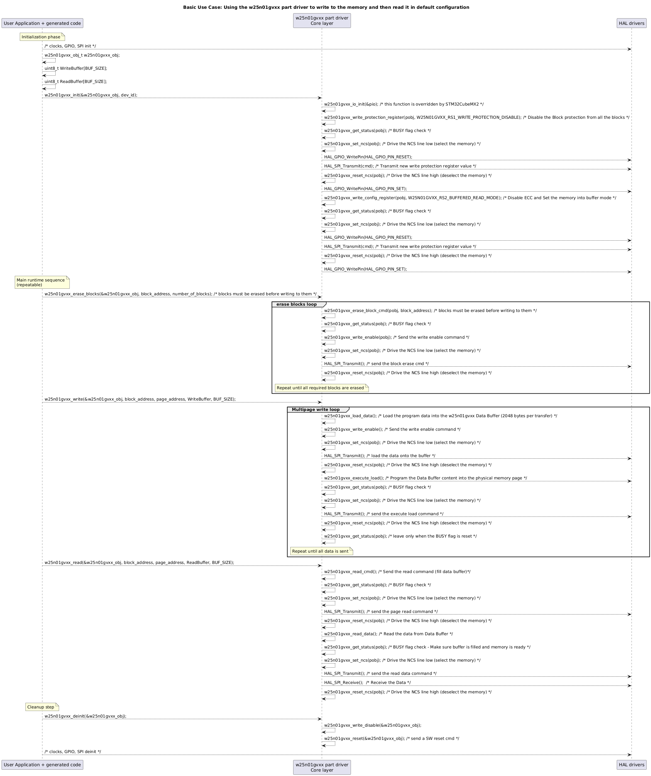
The diagram below presents a simple use case: Using the W25N01GVXX Part Drivers to write to the memory and then read it in default configuration.
The diagram below presents an advanced use case: Using the W25N01GVXX Part Drivers to write to the flash memory and then read it in continuous configuration.
The diagram below presents an advanced use case: Using the W25N01GVXX Part Drivers to write data with DMA which demonstrates the async write sequence.
Dependencies 
The diagram below presents the partitioning of this driver into components.
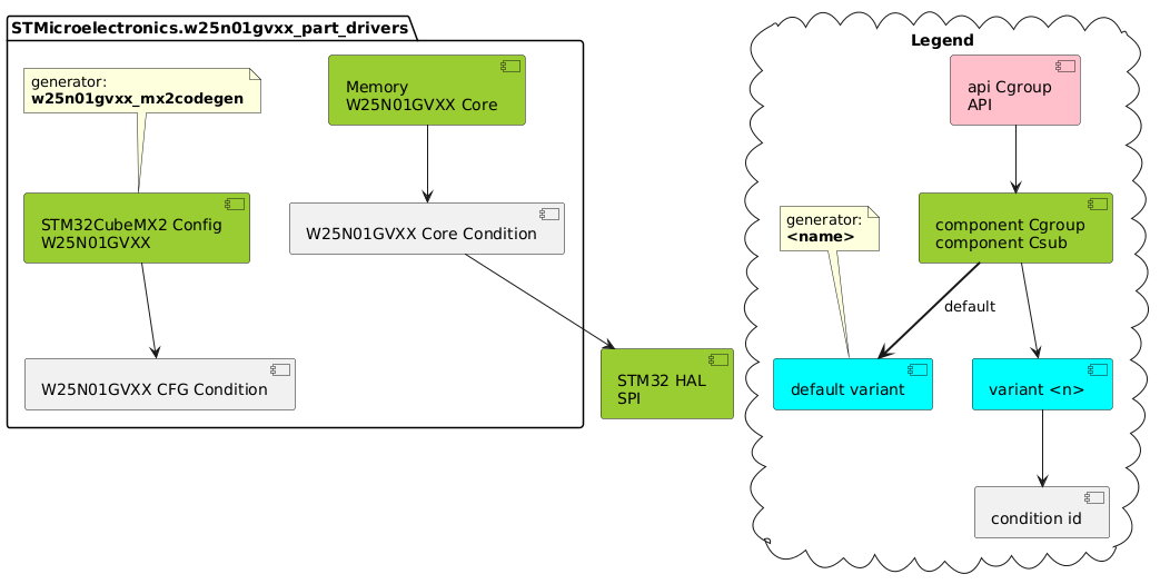
This components’ structure translates to the following inclusion graph in terms of C code: