
4 STM32CubeMX user interface 
STM32CubeMX user interface comes with three main views the user can navigate through using convenient breadcrumbs, namely the Home page, the New project window, and the project page. They come with panels, buttons and menus allowing users to take actions and make configuration choices with a single click.
The user interface is detailed in the following sections.
For C code generation, although the user can switch back and forth between the different configuration views, it is recommended to follow the sequence below:
1. From the Project Manager view, configure the project settings.
2. From the Mode panel in the Pinout & Configuration view, configure the RCC peripheral by enabling the external clocks, master output clocks, audio input clocks (when relevant for your application). This automatically displays more options on the Clock configuration view (see Figure 183). Then, select the features (peripherals, middlewares) and their operating modes relevant to the application.
3. If necessary, adjust the clock tree configuration from the clock configuration view.
4. From the Configuration panel in the Pinout & Configuration view configure the parameters required to initialize the peripherals and middleware operating modes.
5. Generate the initialization C code by clicking .
4.1 Home page
This is the first window that opens up when launching STM32CubeMX (see Figure 33). Closing it closes down the application. It offers shortcuts for some top level menus, an image carousel displaying STM32 latest news, as well as links to social network sites and external tools. Top-level menus and social network links remain accessible from the subsequent project page and are detailed in the following sections.
Figure 33. STM32CubeMX home page

4.1.1 File menu
Refer to Table 2 for a description of the File menu and shortcuts.
Table 2. Home page shortcuts
Name
Keyboard shortcut
Description
Home page shortcut
New Project… Ctrl-N
Opens a new project window showing all supported MCUs and a set of STMicroelectronics boards to choose from(1).
To create a new project starting from a board click
To create a new project starting from an MCU click
Load Project… Ctrl-L
Loads an existing STM32CubeMX project configuration by selecting an STM32CubeMX configuration .ioc file (see Caution:).
Under Other project, click browse icon
Import Project…
Ctrl-I
Opens a new window to select the configuration file to be imported as well as the import settings. The import is possible only if you start from an empty MCU configuration. Otherwise, the menu is disabled(2).
None
Save Project Ctrl-S
Saves current project configuration (pinout, clock tree, peripherals, middlewares, Power Consumption Calculator) as a new project.
This action creates a project folder including an .ioc file, according to user defined project settings.
None
Save Project as… Ctrl-A
Saves the current project.
None
Close Project Ctrl-C
Closes the current project and switches back to the welcome page.
None
Recent Projects none
Displays the list of the five most recently saved projects.
|image39| Under Recent Project, click the project name.
icon next to
Generate Report Ctrl-R
Saves the project current configuration as two documents (pdf and text formats).
None
To close the window and the application click on .
Exit Ctrl-X
Proposes to save the project (if needed), then closes the application.
1. On New project: to avoid any popup error messages at this stage, make sure an Internet connection is available (Connection Parameters tab under Help > Updater settings menu) or that Data Auto-refresh settings are set to No Auto-Refresh at application start (Updater Settings tab under Help > Updater Settings menu).
2. On Import, a status window displays the warnings or errors detected when checking for import conflicts. The user can then decide to cancel the import.
Caution: ** On **project load: STM32CubeMX detects if the project was created with an older version of the tool and if this is the case, it proposes the user to either migrate to use the latest STM32CubeMX database and STM32Cube firmware version, or to continue. Prior to STM32CubeMX 4.17, clicking Continue still upgrades to the latest database “compatible” with the STM32Cube firmware version used by the project.
Starting from STM32CubeMX 4.17, clicking Continue keeps the database used to create the project untouched. If the required database version is not available on the computer, it is automatically downloaded.
When upgrading to a new version of STM32CubeMX, make sure to always backup your projects before loading the new project (especially when the project includes user code).
4.1.2 Window menu and Outputs tabs
The Window menu allows the user to access the Outputs function.
Table 3. Window menu
Name
Description
Outputs
Selecting/deselecting Outputs from the Window menu hides/shows the following
Outputs tabs at the bottom of STM32CubeMX project page (see Figure 34)
– MCUs selection: lists the MCUs of a given family matching the user criteria (series, peripherals, package,…) when an MCU was selected last(1).
– Outputs: displays a non-exhaustive list of the actions performed, raised errors and warnings (see Figure 35) found upon user actions.
– IP assignment rules
– MMT Output Log
Font size
Makes possible to change font size settings. STM32CubeMX must be re-launched for changes to take effect.
1. Selecting a different MCU from the list resets the current project configuration and switches to the new MCU. The user is then prompted to confirm this action before proceeding.
Figure 35. Output view
Refer to Table 4 for a description of the Help menu and shortcuts.
Table 4. Help menu shortcuts
|
Name Keyboard shortcut |
Description |
Home page shortcut |
|
Help F1 |
Opens the STM32CubeMX user manual. |
None |
|
About Alt-A |
Shows version information. |
None |
|
Docs & Resources Alt-D |
Displays the official documentation available for the MCU used in the current project. |
None |
|
Video Tutorials Alt-V |
Opens the Video Tutorial browser that proposes a list of videos and allows the user to launch a video in one click. |
None |
|
Refresh Data Alt-R |
Opens a dialog window that proposes to refresh STM32CubeMX database with STM32 MCU latest information (description and list of official documents), and allows the user to download of all official documentation in one shot. |
None |
|
Check for Updates Alt-C |
Shows the software and firmware release updates available for download. |
Click |
|
Manage embedded software packages Alt-U |
Shows all the embedded software packages available for installation. A green check box indicates that the package is already installed in the user repository folder (the repository folder location is specified under Help > Updater Settings menu). |
Click |
Table 4. Help menu shortcuts (continued)
|
Name Keyboard shortcut |
Description |
Home page shortcut |
|
|
Connection & Updates Alt-S |
Opens the Connection & Updates window to configure manual or automatic updates, proxy settings for Internet connections, and repository folder where the downloaded software and firmware releases are stored. |
None |
|
|
User Preferences |
Opens the user preference window to enable or disable collect of features usage statistics. |
None |
4.1.4 Social links
Developer communities on popular social platforms such as Facebook™, STM32
YouTube™ channel, as well as ST Community can be accessed from the STM32CubeMX toolbar (see Figure 36).

4.2 New Project window
The New Project window is accessible through the File Menu, or directly through shortcuts from the Home page (see Figure 37).
Figure 37. New Project window shortcuts

The main purpose is to select from the STM32 portfolio the microcontroller or board that best fits the user application needs, or simply to get started using an example project.
This window shows three tabs to choose from:
• an MCU selector tab (offering a list of target processors)
• a Board selector tab (showing a list of STMicroelectronics boards)
• an Example selector tab (allows the user to browse and open an example project)
The new project window also features a Cross selector tab (allows the user to find, for a given MCU/MPU part number and for a set of criteria, the best replacement within the STM32 portfolio)
For the STM32L5 series the security features of the Arm Cortex-M33 processor and its Arm ® TrustZone ®(a) for Armv8-M are combined with ST security implementation. Selecting an STM32L5 MCU or board requires to choose whether to activate Arm ® TrustZone ® (hardware security) or not (see Figure 38). The project is adjusted accordingly:
• if Arm ® TrustZone ® is not activated, the solution is the same as for other STM32Lx series
a. Arm and TrustZone are registered trademarks of Arm Limited (or its subsidiaries or affiliates) in the US and/or elsewhere.
• if Arm ® TrustZone ® is activated, the project configuration and the generated project shows specificities related to the security features (refer to dedicated sections in this manual).
The selectors result view can be adjusted (see Figure 39):
• Left click the column to sort
• Right click to add/remove columns
4.2.1 MCU selector
MCU selection
The MCU selector enables filtering on a combination of criteria: series, lines, packages, peripherals, or additional characteristics such as price, memory size, number of I/Os (see Figure 40), and on their graphics capabilities as well.
Figure 40. New Project window - MCU selector


4.2.2 Board selector
The Board selector enables filtering on STM32 board types, series and peripherals (see Figure 42). Only the default board configuration is proposed. Alternative board configurations obtained by reconfiguring jumpers or by using solder bridges are not supported.
When a board is selected, the Pinout view is initialized with the relevant MCU part number along with the pin assignments for the LCD, buttons, communication interfaces, LEDs, and other functions. Optionally, the user can choose to initialize it with the default peripheral modes.
When a board configuration is selected, the signals change to “pinned”, that is, they cannot be moved automatically by STM32CubeMX constraint solver (an user action on the peripheral tree, such as the selection of a peripheral mode, does not move the signals). This ensures that the user configuration remains compatible with the board.
Figure 42. New Project window - Board selector

The Example selector allows the user to browse a large set of examples and to start a new project from a selected example.
Note: An example is always related to a specific board, and, consequently, for the MCU available with that board.
Thanks to the filter panel it is possible to filter down the example list for a specific board type, series, peripheral or middleware as well as other characteristics (see Figure 43).
Figure 43. New project window - Example selector

Selecting an example and clicking “Start project” allows STM32CubeMX to copy the example as a new project (the user can change the default location at this stage).
Warning: For some examples the “Start Project” button is shown with an “Under Development” warning icon. Projects created from these examples may be not functional (they do not compile). Fixes are in development.
Several options are available to open the newly created project (see Figure 44): - with STM32CubeMX (available only for examples listed with an STM32CubeMX version set)
• with a File explorer
• with one of the supported toolchains (provided the toolchain is already installed on your computer)
Figure 44. Popup window - Starting a project from an example

Note: If the STM32Cube MCU package needed for the example is missing from the repository, STM32CubeMX automatically starts the download process.
4.2.4 Cross selector
Part number selection
The Cross selector allows users to find the products that best replace the MCU or MPU they are currently using (from ST or other silicon vendors).
To access this functionality, STM32CubeMX data must be up to date. This is ensured using Refresh Data from the Help menu (see Figure 45).
Figure 45. Cross selector - Data refresh prerequisite

Clicking “ACCESS TO CROSS SELECTOR” under the “Start my project from Cross Selector” section of the main page opens the New Project window on the Cross selector tab.
Two drop downs menus allow the user to select the vendor and the part number of the product to be compared to (see Figure 46). A part number can also be entered partially: STM32CubeMX proposes a list of matching products (see Figure 47).
Figure 46. Cross selector - Part number selection per vendor

Compare cart
Once a part number is selected, a list of matching ST part number candidates is displayed along with their matching ratio in the Matching ST candidates panel.
By default, the three closest matches are selected and added to the compare cart along with the part number to be compared to (see Figure 48).
Figure 48. Cross selector - Compare cart

This selection can be changed anytime in the Matching ST candidates panel.
The comparison can be customized: the features to be used for comparison can be unselected when considered as irrelevant and their level of importance can be adjusted. These choices affect the computed matching ratio.
The comparison is disabled for features that are not supported on the part number to be compared with, or when the feature information is unavailable.
Buttons are available to manipulate and save a copy of the compare cart view:
• to hide criteria not used for the comparison, or show all of them
• to come back to default STM32CubeMX comparison settings • to copy and paste the current cart view in a document or email.
MCU/MPU selection for a new project
Clicking an STM32 part number from the compare cart selects it in the MCU/MPU Selector tab, and clicking on creates a new project for that part number (see Figure 49).
Figure 49. Cross selector - Part number selection for a new project

Clicking the Cross Selector Tab allows the user to go back to the cart and change the current selection for another part number.
4.3 Project page
Once an STM32 part number or a board has been selected or a previously saved project has been loaded, the project page opens, showing the following set of views (refer to dedicated sections for their detailed description):
• Pinout & Configuration • Clock Configuration • Project Manager • Tools
Users can move across the different views without impacting their project configuration.
A button is always accessible for the user to click and allows to
generate the code corresponding to the current project configuration. Moreover, thanks to convenient navigation breadcrumbs (see Figure 50), the user can detect what its current location is in STM32CubeMX user interface, and can move to other locations:
• to the home page by clicking the Home breadcrumb
• to the new project window by clicking the part number
• back to the project page by clicking the project name (or Untitled if the project does not have a name yet).
Figure 50. STM32CubeMX Main window upon MCU selection

Selecting a board, then answering No in the dialog window requesting to initialize all peripherals to their default mode, automatically sets the pinout for this board. However, only the pins set as GPIOs are marked as configured, i.e. highlighted in green, while no peripheral mode is set. The user can then manually select from the peripheral tree the peripheral modes required for its application (see Figure 51).
Figure 51. STM32CubeMX Main window upon board selection (peripherals not initialized)

Selecting a board and accepting to initialize all peripherals to their default mode automatically sets both the pinout and the default modes for the peripherals available on the board. This means that STM32CubeMX generates the C initialization code for all the peripherals available on the board and not only for those relevant to the user application (see Figure 52).
Figure 52. STM32CubeMX Main window upon board selection (peripherals initialized with default configuration)

4.4 Boot chain (STM32 MPUs)
4.4.1 Boot mode configuration
ST embedded software can support complex architectures (such as OpenSTLinux), which require a complex boot chain, involving several processors, firmware, and a complex boot sequence. An overview is given in the STM32MPU Wiki portal.
The boot mode defines the processor that starts the software, defines the boot sequence scheme, and which software services can be started (such as secure services, also known as TrustZone ® ).
Creating a project for a dual core (Cortex-A35 and Cortex-M33) MPU
The first example uses the following boot mode: Cortex-A35 is the master processor, Cortex-M33 is the secondary one, in non-secure mode.
The master always runs in a secure mode.
• Select an STM32MP257x MPU
• Select the option “with A35 Master without Cortex M33 TrustZone activated?” on the popup window (see Figure 53)
• Six contexts are created in the configuration panel (see Figure 54)
Figure 54. Contexts

• The Cortex-A35 runs under the OpenSTLinux operating system. It uses the following firmware:
– TF-A BL2
– OP-TEE
– U-Boot
– Linux
• The Cortex-M33 is configured using Cube firmware: M33NS Cube FW (HAL & LL) Figure 55. IPs interface assignment

After assigning the IPs context go to “Project Manager” view, save the project, and generate the code.
The second example uses the following boot mode: Cortex-A35 is the master processor, Cortex-M33 core is the secondary one, in secure mode.
The master always runs in a secure mode.
• Select an STM32MP257x MPU
• Select the option “with A35 Master with Cortex M33 TrustZone activated?” on the popup window (see Figure 56)
• Six contexts created in the configuration panel (see Figure 57)
Figure 57. Selected context

Cortex-A35 runs under the OpenSTLinux operating system. It uses the following firmware:
– TF-A BL2
– OP-TEE
– U-Boot
– Linux
Cortex-M33 secure is configured using Cube firmware: TF-M
To assign IPs context go to “Pinout & Configuration” and configure IPs.
Figure 58. Assign IP context

After assigning the IPs context go to “Project Manager” view, save the project, and then generate code.
4.4.2 Coprocessor initializers (STM32MP2x)
The STM32MP2xx comes with two possible coprocessors (Cortex-M33 or Cortex-M0+). STM32CubeMX manages only Cortex-M33.
The STM32CubeMX tool indicates which programs running on the main processor can be started, or if to use the secondary processor.
When the system source code is generated, the settings that determine how the main processor can use the coprocessor are included in the device tree. These settings are found in the “rproc” sections (nodes) for each software component that can interact with the coprocessor. This ensures that, when the system is running, it knows how to handle the coprocessor according to the predefined configuration.
As an example:
• OP-TEE is eligible to load the main processor.
• Linux Kernel is eligible to load for the main processor.
• U-Boot will be available when Linux is selected. Figure 60. U-Boot selection

4.4.3 Boot device selection (STM32MP25)
The term boot device refers to any storage device from which a microcontroller can load the initial software used to boot up the system. This initial software is part of the boot process that starts the computer and loads the operating system.
STM32CubeMX does not handle the configuration of the pins used by STM32 devices to select the boot source. To configure a correct boot, ensure that the boot device settings align with the boot pins configuration, programmed in the MCU hardware. This requires checking the datasheet or reference manual, to understand the boot pin settings, and then manually configuring the system to match those settings.
A boot device must be assigned to the ROM firmware and the early-stage Boot Loader (such as TF-A BL2 for OpenSTLinux).
When configuring a microcontroller, consider the constraints that affect the choice of boot devices, and their dependency upon the selected boot mode. STM32CubeMX checks the boot configuration of against a set of constraints to ensure that the system boots properly. This service is called Flexible Software Loader synchronization verification. The results of this verification are displayed in a dedicated output window (FSBL synchro output), providing developers with important diagnostic information.
The “FSBL synchro output” panel is displayed with the rule “Faulty state detected for SDMMC1: FSBL-A assignments possible only if assigned in BootRom”. Users can refer to this panel to align any misconfigurations.
Figure 61. FSBL synchronization output

4.5 Pinout & Configuration view
The Pinout & Configuration view comes with the following main panels, function and menu:
• A Component list that can be visualized in alphabetical order and per categories. By default, it consists of the list of peripheral and middleware that the selected MCU supports. Selecting a component from that list opens two additional panels ( Mode and Configuration) that allow the user to set its functional mode and configure the initialization parameters that will be included in the generated code.
• A Pinout view that shows a graphic representation of the pinout for the selected package (e.g. BGA, QFP) where each pin is represented with its name (e.g. PC4) and its current alternate function assignment, if any.
• A System view that gives an overview of all the software configurable components: GPIOs, peripherals, middleware and additional software components. Clickable buttons allow opening the configuration options for the given component (Mode and Configuration panels). The button icon color reflects the status of the configuration status.
• A Software Packs menu with two sub-menus:
– Select Components to select, for the current project, software components not available by default. This selection updates the Pinout & Configuration view accordingly
– Manage Software Packs to install/uninstall software packs.
• An Additional Software function that allows to select, for the current project, software components that are not available by default. Selecting an additional software component updates the Pinout & Configuration view accordingly.
• A Pinout menu that allows the user to perform pinout related actions such as clear pinout configuration or export pinout configuration as csv file.
Tips
• You can resize the panels: hovering the mouse over a panel border displays a two-ended arrow: right-click and pull in a direction to extend or reduce the panel.
• You can show/hide the Configuration, Mode, Pinout and System views using the open and close arrows.
4.5.1 Component list
The component list shows all the components available for the project. Selecting a component from the component list, opens the Mode and Configuration panels.
Contextual help
The Contextual Help window is displayed when hovering the mouse over a peripheral or a middleware short name.
By default, the window displays the extended name and source of configuration conflicts if any (see Figure 62).
Clicking the details and documentation link (or CTRL+d) provides additional information such as summary and reference documentation links (see Figure 63). For a given peripheral, clicking Datasheet or Reference manual opens the corresponding document, stored in STM32CubeMX repository folder, at the relevant chapter. Since microcontrollers datasheets and reference manuals are downloaded to STM32CubeMX repository only upon user request, a functional Internet connection is required:
• To check your Internet connection, open the Connection tab from the Help > Updater Settings menu.
• To request the download of reference documentation for the currently selected microcontroller, click Refresh from the Help > Refresh Data menu window.
Figure 63. Contextual Help detailed information

Icons and color schemes
Table 5 shows the icons and color scheme used in the component list view and the corresponding color scheme in the Mode panel.
Table 5. Component list, mode icons and color schemes
|
Display |
Component status |
Corresponding Mode view / Tooltips |
|
Plain black text Example: |
The peripheral is not configured (no mode is set) and all modes are available. |
|
|
Gray italic text Example: |
Peripheral is not available because some constraints are not solved. See tooltip. |
|
|
Example: |
The peripheral is configured (at least one mode is set) and all other modes are available. The green check mark indicates that all parameters are properly configured, a cross indicates they are not. |
Table 5. Component list, mode icons and color schemes (continued)
|
Display |
Component status |
Corresponding Mode view / Tooltips |
|
Example: |
The peripheral is not configured (no mode is set) and at least one of its modes is unavailable. |
|
|
Example: |
The peripheral is configured (one mode is set) and at least one of its other modes is unavailable. |
|
|
Example: |
The peripheral is not configured (no mode is set) and no mode is available. Move the mouse over the peripheral name to display the tooltip describing the conflict. |
|
|
Example: IRTIM |
Peripheral is not available because of constraints. |
4.5.2 Component Mode panel
Select a component from the component list on the left panel to open the Mode panel.
The Mode panel helps the user configuring the MCU pins based on a selection of peripherals and of their operating modes. Since STM32 MCUs allow a same pin to be used by different peripherals and for several functions (alternate functions), the tool searches for the pinout configuration that best fits the set of peripherals selected by the user. STM32CubeMX highlights the conflicts that cannot be solved automatically (see Table 5).
The Mode panel also allows to enable middleware and other software components for the project.
Note: For some middleware (USB, FATS, LwIP), a peripheral mode must be enabled before activating the middleware mode. Tooltips guide the user through the configuration. For FatFs, a user-defined mode has been introduced. This allows STM32CubeMX to generate FatFs code without a predefined peripheral mode. Then, it is up to the user to connect the middleware with a user-defined peripheral by updating the generated user_diskio.c/.h driver files with the necessary code.
4.5.3 Pinout view
Select to show for the selected part number, a graphic representation of the pinout for the selected package (such as. BGA, QFP), where each pin is represented with its name (such as PC4), its configuration state and its current alternate function assignment, if any (such as ETH_MII_RXD0). See Figure 64 for an example.
Figure 64. Pinout view

The Pinout view is automatically refreshed to match the user’s component configuration performed in the Mode panel.
Assigning pins directly through the Pinout view instead of the Mode panel requires a good knowledge of the MCU since each individual pin can be assigned to a specific function.
Tips and tricks
See Table 2 for list of menus and shortcuts.
• Use the mouse wheel to zoom in and out.
• Click and drag the chip diagram to move it.
• Click best fit to reset it to best suited position and size. • Use Pinout > Export pinout menus to export the pinout configuration as .csv text format.
• Some basic controls, such as insuring consistency for blocks of pins, are built-in. See Appendix A for details.
4.5.4 Pinout menu and shortcuts
Table 6. Pinout menu and shortcuts
|
Name or Icon |
Shortcut |
Description |
|
Keep Current Signals Placement |
Ctrl-K |
Prevents moving pin assignments to match a new peripheral operating mode. It is recommended to use the new pinning feature that can block each pin assignment individually and leave this checkbox unchecked. |
|
Show User Label |
None |
Displays user defined labels in the Pinout view. |
|
Undo Mode and pinout |
Ctrl-Z |
Undoes last configuration steps (one by one). |
|
Redo Mode and pinout |
Ctrl-Y |
Redoes steps that have been undone (one by one). Warning (limitation): configurations in the platform settings tabs are not restored. |
|
Disable All Modes |
Ctrl-D |
Resets to “Disabled” all peripherals and middleware modes that have been enabled. The pins configured in these modes (green color) are consequently reset to “Unused” (gray color). Peripheral and middleware labels change from green to black (when unused) or gray (when not available). |
|
Clear Pinouts |
Ctrl-P |
Clears user pinout configuration in the Pinout view. Note that this action puts all configured pins back to their reset state and disables all the peripheral and middleware modes previously enabled (whether they were using signals on pins or not). |
|
Pins/Signals Option |
Ctrl-O |
Opens a window showing the list of all the configured pins together with the name of the signal on the pin and a Label field allowing the user to specify a label name for each pin of the list. For this menu to be active, at least one pin must have been configured. Click the pin icon to pin/unpin signals individually. Select multiple rows then right click to open contextual menu and select action to pin or unpin all selected signals at once. Click column header names to sort alphabetically by name or according to placement on MCU. |
|
Clear Single Mapped Signals |
Ctrl-M |
Clears signal assignments to pins for signals that have no associated mode (highlighted in orange and not pinned). |
Table 6. Pinout menu and shortcuts (continued)
|
Name or Icon |
Shortcut |
Description |
|
List Pinout Compatible MCUs |
Alt-L |
Provides a list of MCUs that best match the pin configuration of the current project. The matching can be: – An exact match – A partial match with hardware compatibility: pin locations are the same, pin names may have been changed – A partial match without hardware compatibility: all signals can be mapped but not all at the same pin location Refer to Section 15. |
|
Export pinout with Alternate functions |
|
Generates pin configuration as a .csv text file including alternate functions information. |
|
Export pinout without Alternate functions |
Ctrl-U |
Generates pin configuration as a .csv text file excluding alternate functions information. |
|
Reset used GPIOs |
Alt-G |
Opens a window to specify the number of GPIOs to be freed among the total number of GPIO pins that are configured. |
|
Set unused GPIOs |
Ctrl-G |
Opens a window to specify the number of GPIOs to be configured among the total number of GPIO pins that are not used yet. Specify their mode: Input, Output or Analog (recommended configuration to optimize power consumption). Caution: Before using this menu, make sure that debug pins (available under SYS peripheral) are set to access microcontroller debug facilities. |
|
Layout reset |
|
|
|
|
Zooms-in the pinout view. |
|
|
|
Adjusts the chip pinout diagram to the best fit size. |
|
|
|
Zooms-out the pinout view. |
|
|
|
Rotates 90 degrees clock wise. |
|
|
|
Rotate 90 degrees counter-clock wise. |
|
|
|
Flips horizontally between bottom view and top view. |
|
|
|
Flips vertically between bottom view and top view. |
|
|
|
This Search field allows the user to search the Pinout view for a pin name, a signal name, a signal label or an alternate pin name When it is found, the pin or set of pins matching the search criteria blinks on the Pinout view. Click the Pinout view to stop blinking. |
4.5.5 Pinout view advanced actions
Manually modifying pin assignments
To manually modify a pin assignment, follow the sequence below:
1. Click the pin in the Pinout view to display the list of all other possible alternate functions together with the current assignment highlighted in blue (see Figure 65).
2. Click to select the new function to assign to the pin.
Figure 65. Modifying pin assignments from the Pinout view

|
Manually remapping a function to another pin To manually remap a function to another pin, follow the sequence below: 1. From the Pinout view, hold down the CTRL key then left-click on the pin and hold: if any pins are possible for relocation, they are highlighted in blue and blinking. 2. Drag the function to the target pin. |
|
|
Caution: |
A pin assignment performed from the Pinout view overwrites any previous assignment. Manual remapping with destination pin ambiguity For MCUs with block of pins consistency (STM32F100x / F101x / F102x / F103x and STM32F105x / F107x), the destination pin can be ambiguous, e.g. there can be more than one destination block including the destination pin. To display all the possible alternative remapping blocks, move the mouse over the target pin. |
|
Note: |
A “block of pins” is a group of pins that must be assigned together to achieve a given |
peripheral mode. As shown in Figure 66, two blocks of pins are available on STM32F107xx MCUs to configure the Ethernet peripheral in RMII synchronous mode: {PC1, PA1, PA2, PA7, PC4, PC5, PB11, PB12, PB13, PB5} and {PC1, PA1, PA2, PD10, PD9, PD8, PB11, PB12, PB13, PB5}.
Figure 66. Example of remapping in case of block of pins consistency
To resolve the pin conflicts that may occur when some peripheral modes use the same pins, STM32CubeMX attempts to reassign the peripheral mode functions to other pins. The peripherals for which pin conflicts cannot be solved are highlighted in fuchsia with a tooltip describing the conflict.
If the conflict cannot be solved by remapping the modes, the user can try the following:
• If the ** ** box is checked, try to select the peripherals in a different sequence.
• Uncheck the Keep Current Signals Placement box and let STM32CubeMX try all the remap combinations to find a solution.
• Manually remap a mode of a peripheral when you cannot use it because there is no pin available for one of the signals of that mode.
4.5.6 Keep Current Signals Placement
This checkbox is available from the Pinout menu. It can be selected or deselected at any time during the configuration. It is unselected by default.
It is recommended to keep the checkbox unchecked for an optimized placement of the peripherals (maximum number of peripherals concurrently used).
The Keep Current Signals Placement checkbox should be selected when the objective is to match a board design.
Keep Current Signals Placement is unchecked
This allows STM32CubeMX to remap previously mapped blocks to other pins in order to serve a new request (selection of a new peripheral mode or a new peripheral mode function) which conflicts with the current pinout configuration.
Keep Current Signals Placement is checked
This ensures that all the functions corresponding to a given peripheral mode remain allocated (mapped) to a given pin. Once the allocation is done, STM32CubeMX cannot move a peripheral mode function from one pin to another. New configuration requests are served if feasible within current pin configuration.
This functionality is useful to:
• lock all the pins corresponding to peripherals that have been configured using the Peripherals panel
• maintain a function mapped to a pin while doing manual remapping from the Pinout view.
Tip
If a mode becomes unavailable (highlighted in fuchsia), try to find another pin remapping configuration for this mode by following the steps below:
1. From the Pinout view, deselect the assigned functions one by one until the mode becomes available again.
2. Then, select the mode again and continue the pinout configuration with the new sequence (see Appendix A: STM32CubeMX pin assignment rules for a remapping example). This operation being time consuming, it is recommended to deselect the Keep Current Signals Placement checkbox.
Note: Even if Keep Current Signals Placement is unchecked, GPIO_ functions (excepted GPIO_EXTI functions) are not moved by STM32CubeMX.
4.5.7 Pinning and labeling signals on pins
STM32CubeMX comes with a feature allowing the user to selectively lock (or pin) signals to pins. This prevents STM32CubeMX from automatically moving pinned signals to other pins when resolving conflicts. Labels, that are used for code generation, can also be assigned to the signals (see Section 6.1 for details).
There are several ways to pin, unpin and label the signals:
1. From the Pinout view, right-click a pin with a signal assignment. This opens a contextual menu:
a) For unpinned signals, select Signal Pinning to pin the signal. A pin icon is then displayed on the relevant pin. The signal can no longer be moved automatically (for example when resolving pin assignment conflicts).
b) For pinned signals, select Signal Unpinning to unpin the signal. The pin icon is removed. From now on, to resolve a conflict (such as peripheral mode conflict), this signal can be moved to another pin, provided the Keep user placement option is unchecked.
c) Select Enter User Label to specify a user defined label for this signal. The new label replaces the default signal name in the Pinout view.
2. From the Pinout menu, select Pins/Signals Options
The Pins/Signals Options window (see Figure 67) lists all configured pins.
Figure 67. Pins/Signals Options window
a) Click the first column to individually pin/unpin signals.
b) Select multiple rows and right-click to open the contextual menu and select Signal(s) Pinning or Unpinning.
c) Select the User Label field to edit the field and enter a user-defined label.
d) Order list alphabetically by Pin or Signal name by clicking the column header. Click once more to go back to default i.e. to list ordered according to pin placement on MCU.
Note: Even if a signal is pinned, it is still possible however to manually change the pin signal assignment from the Pinout view: click the pin to display other possible signals for this pin and select the relevant one.
4.5.8 Pinout for multi-bonding packages
Multi-bonding has been introduced for packages with low pin counts (less than 20 pins) such as SO8N, TSSOP20 and WLCSP18 packages. it consists of having several MCU pads share a same pin on the package.
Multi-bonding has been introduced on the STM32G0 series for the STM32G031/G041 MCUs.
STM32CubeMX pinout view allows to displays all signals arriving on the pin and allows to select only one per pin, except for analog signals that can be combined with other analog GPIOs.
Figure 68. Pinout view: MCUs with multi-bonding
STM32CUbeMX offers also an extended mode selected by right-clicking the pin: it allows to select more than one signal per pin. This mode is meant for test purposes such as loopback tests. It is to be used with caution as it can lead to electrical conflicts or increased power consumption that can damage the device.
Figure 69. Pinout view: multi-bonding with extended mode
4.5.9 System view
Select to show all the software configurable components: GPIOs,
peripherals and middleware. Clickable buttons allow the user to open the mode and configuration options of the component. The button icon reflects the component configuration status (see Table 7 for configuration states and Figure System view).
When the user changes the component configuration from the Configuration panel, the system view is automatically refreshed with the new configuration state.
If the user disables the component from the Mode panel, the system view is automatically refreshed and there is no longer a button showing for that component.
Figure 70. System view
Table 7. Configuration states
|
Icon |
Description |
|
Configuration is complete and correct. |
|
|
Configuration is correct but some parts remain to be configured (optional). |
|
|
Configuration is invalid and must be fixed for the generated C project to be functional. |
GPIO, DMA and NVIC settings can be accessed either via a dedicated button (like other peripherals, or via a tab in the Configuration panel (see Figure 71).
Figure 71. Configuration window tabs (GPIO, DMA, and NVIC settings for STM32F4 series)
4.5.10 Component configuration panel
This panel appears when clicking on a component name in the left panel. It allows the user to configure the functional parameters required to initialize the peripheral or the middleware in the selected operating mode (see Figure 72). STM32CubeMX uses these settings to generate the corresponding initialization C code.
The configuration window includes several tabs:
• Parameter settings to configure library dedicated parameters for the selected peripheral or middleware,
• NVIC, GPIO and DMA settings to set the parameters for the selected peripheral (see Section 4.5.14, Section 4.5.12 and Section 4.5.13).
• User constants to create one or several user defined constants, common to the whole project (see Section 4.5.11).
Invalid settings are detected and are:
• reset to minimum / maximum valid value if user choice is, respectively, smaller / larger than minimum / maximum threshold
• reset to the previous valid value if the previous one is neither a maximum nor a minimum threshold value
• highlighted in fuchsia.
Figure 72. Peripheral mode and Configuration view
Table 8 describes peripheral and middleware configuration buttons and messages.
Table 8. Peripheral and Middleware configuration window buttons and tooltips
|
Buttons and messages |
Action |
|
Shows / hides the description panel. |
|
|
Tooltip |
Guides the user through the settings of parameters with valid min-max range. To display it, move the mouse over a parameter value from a list of possible values. |
|
Clicking on the gear icon allows to select whether to display hexadecimal or decimal values, or any value unchecked (No check option). |
|
|
Search |
|
|
Resets the component back to its default configuration (initial settings from STM32CubeMX). |
No check option
By default, STM32CubeMX checks that the parameter values entered by the user are valid. This check can be bypassed by selecting the option No Check for a given parameter. This
allows entering you any value (such as a constant) that might not be known by STM32CubeMX configuration.
The validity check can be bypassed only on parameters whose values are of integer type (either hexadecimal or decimal). It cannot be bypassed on parameters coming from a predefined list of possible values or on those which are of non-integer or text type.
To go back to the default mode (decimal or hexadecimal values with validity check enabled), enter a decimal or hexadecimal value and check the relevant option (hexadecimal or decimal check).
** Caution: ** When a parameter depends upon another parameter that is set to No Check:
• Case of a parameter depending on another parameter for the evaluation of its minimum or maximum possible value: If the other parameter is set to No Check, the minimum or maximum value is no longer evaluated and checked.
• Case of a parameter depending on another parameter for the evaluation of its current value: If the other parameter is set to No Check, the value is no longer automatically derived. Instead, it is replaced with the formula text showing as variable the string of the parameter set to No check (see Figure 73).
Figure 73. Formula when input parameter is set in No Check mode
4.5.11 User Constants configuration window
The User Constants tab is available to define user constants (see Figure 74). Constants are automatically generated in the STM32CubeMX user project within the main.h file (see Figure 75). Once defined, they can be used to configure peripheral and middleware parameters (see Figure 76).
Figure 76. Using constants for peripheral parameter settings
Click the Add button to open the User Constants tab and create a new user-defined constant (see Figure 77).
A constant consists of:
• A name that must comply with the following rules:
– It must be unique.
– It must not be a C/C++ keyword.
– It must not contain a space.
– It must not start with digits.
• A value, which can be (see Figure 74 for examples):
– a simple decimal or hexadecimal value
– a previously defined constant
– a formula using arithmetic operators (subtraction, addition, division, multiplication, and remainder) and numeric value or user-defined numeric constants as operands
– a character string: the string value must be between double quotes (example: “constant_for_usart”).
Once a constant is defined, its name and/or value can be changed: double-click the row that specifies the user constant to modify. This opens the User Constants tab for edition. The change of constant name is applied wherever the constant is used. This does not affect the peripheral or middleware configuration state. Changing the constant value impacts the parameters that use it and might result in invalid settings (such as exceeding a maximum threshold). Invalid parameter settings are highlighted in fuchsia.
Figure 77. Specifying user constant value and name
Click the Remove button to delete an existing user-defined constant.
The user constant is then automatically removed except in the following cases:
• When the constant is used for the definition of another constant. In this case, a popup window displays an explanatory message (see Figure 78).
Figure 78. Deleting an user constant is not allowed when it is already used for another constant definition
• When the constant is used for the configuration of a peripheral or middleware library parameter. In this case, the user is requested to confirm the deletion since the constant removal results in a invalid peripheral or middleware configuration (see Figure 79).
Figure 79. Confirmation request to delete a constant for parameter configuration
Clicking Yes leads to an invalid peripheral configuration (see Figure 80).
Figure 80. Consequence when deleting a user constant for peripheral configuration
The Search Constants field makes it possible the search of a constant name or value in the complete list of user constants (see Figure 81 and Figure 82).
Figure 81. Searching for a name in a user constant list
4.5.12 GPIO configuration window
Click GPIO in the System view panel to open the GPIO configuration window to configure the GPIO pin settings (see Figure 83). The configuration is populated with default values that might not be adequate for some peripheral configurations. In particular, check if the GPIO speed is sufficient for the peripheral communication speed, and select the internal pull-up whenever needed.
Note: GPIO settings can be accessed for a specific peripheral instance via the dedicated window in the peripheral instance configuration window. In addition, GPIOs can be configured in output mode (default output level). The generated code is updated accordingly.
Figure 83. GPIO configuration window - GPIO selection
Click on a row or select a set of rows to display the corresponding GPIO parameters:
• GPIO PIN state
Changes the default value of the GPIO output level. It is set to low by default and can be changed to high.
• GPIO mode (analog, input, output, alternate function)
Selecting a peripheral mode in the Pinout view automatically configures the pins with the relevant alternate function and GPIO mode.
• GPIO pull-up/pull-down
Set to a default value, can be configured when other choices are possible.
• GPIO maximum output speed (for communication peripherals only)
Set to Low by default for power consumption optimization, can be changed to a higher frequency to fit application requirements.
• User Label
Changes the default name (such as GPIO_input) into a user defined name. The Pinout view is updated accordingly. The GPIO can be found under this new name via the Find menu.
The Group by Peripherals checkbox allows the user to group all instances of a peripheral under the same window (see Figure 84).
Figure 84. GPIO configuration grouped by peripheral
As shown in Figure 85, r ow multi-selection can be performed to change a set of pins to a given configuration at the same time.
4.5.13 DMA configuration window
Click DMA in the System view to open the DMA configuration window.
This window is used to configure the generic DMA controllers available on the MCU. The DMA interfaces allow to perform data transfers between memories and peripherals while the CPU is running, and memory to memory transfers (if supported).
Note: Some peripherals (such as USB or Ethernet ) have their own DMA controller, which is enabled by default or via the Peripheral Configuration window.
Clicking Add in the DMA configuration window adds a new line at the end of the DMA configuration window with a combo box proposing to choose between possible DMA requests to be mapped to peripherals signals (see Figure 86).
Figure 86. Adding a new DMA request
Selecting a DMA request automatically assigns a stream among all the streams available, a direction and a priority. When the DMA channel is configured, it is up to the application code to fully describe the DMA transfer run-time parameters such as the start address.
The DMA request (called channel for STM32F4 MCUs) is used to reserve a stream to transfer data between peripherals and memories (see Figure 87). The stream priority is used to decide which stream to select for the next DMA transfer.
DMA controllers support a dual priority system using the software priority first, and in case of equal software priorities, a hardware priority that is given by the stream number.
Figure 87. DMA configuration
Additional DMA configuration settings can be done through the DMA configuration window:
• Mode: regular mode, circular mode, or peripheral flow controller mode (only available for the SDIO peripheral).
• Increment Add: the type of peripheral address and memory address increment (fixed or postincremented, in which case the address is incremented after each transfer). Click the checkbox to enable the post-incremented mode.
• Peripheral data width: 8, 16, or 32 bits
• Switching from the default direct mode to the FIFO mode with programmable threshold:
a) Click the Use FIFO checkbox.
b) Configure the peripheral and memory data width (8, 16, or 32 bits).
c) Select between single transfer and burst transfer. If you select burst transfer, choose a burst size (1, 4, 8, or 16).
In case of memory-to-memory transfer (MemToMem), the DMA configuration applies to a source memory and to a destination memory.
Figure 88. DMA MemToMem configuration
Click NVIC in the System view to open the Nested Vector interrupt controller configuration window (see Figure 89).
Interrupt unmasking and interrupt handlers are managed within two tabs:
• NVIC, to enable peripheral interrupts in the NVIC controller and to set their priorities
• Code generation, to select options for interrupt related code generation
Enabling interruptions using the NVIC tab view
The NVIC view (see Figure 89) does not show all possible interrupts, but only the ones available for the peripherals selected in the Pinout & Configuration panels. System interrupts are displayed but can never be disabled.
Check/uncheck the Show only enabled interrupts box to filter or not enabled interrupts.
When DMA channels are configured in the project, check/uncheck “Force DMA channels interrupts” to automatically enable/disable DMA channels interrupts in the generated code.
Use the search field to filter out the interrupt vector table according to a string value. As an example, after enabling UART peripherals from the Pinout panel, type UART in the NVIC search field and click the green arrow close to it: all UART interrupts are displayed.
Enabling a peripheral interrupt generates NVIC function calls HAL_NVIC_SetPriority and HAL_NVIC_EnableIRQ for this peripheral.
Figure 89. NVIC configuration tab - FreeRTOS disabled
When FreeRTOS is enabled, an additional column is shown (see Figure 90).
In this case, all the interrupt service routines (ISRs) that are calling the interrupt safe
FreeRTOS APIs must have a priority lower than the priority defined in the
LIBRARY_MAX_SYSCALL_INTERRUPT_PRIORITY parameter (the highest the value, the lowest the priority). The check in the corresponding checkbox guarantees that the restriction is applied.
If an ISR does not use such functions, the checkbox can be unchecked and any priority level can be set. It is possible to check/uncheck multiple rows (see rows highlighted in blue in Figure 90).
Figure 90. NVIC configuration tab - FreeRTOS enabled
Peripheral dedicated interrupts can also be accessed through the NVIC window in the configuration window (see Figure 91).
STM32CubeMX NVIC configuration consists in selecting a priority group, enabling/disabling interrupts and configuring interrupts priority levels (preemption and sub-priority levels):
1. Select a priority group
Several bits allow to define NVIC priority levels, they are divided in two groups, preemption priority and sub-priority. For example, in the case of STM32F4 MCUs, the NVIC priority group 0 corresponds to 0-bit preemption and 4-bit sub-priority.
In the interrupt table, click one or more rows to select one or more interrupt vectors. Use the widgets below the interrupt table to configure the vectors one by one or several at a time:
– Enable checkbox: check/uncheck to enable/disable the interrupt.
– Preemption priority: select a priority level. The preemption priority defines the ability of one interrupt to interrupt another.
– Sub-priority: select a priority level. Defines the interrupt priority level.
Code generation options for interrupt handling
The Code Generation view allows customizing the code generated for interrupt initialization and interrupt handlers: - Selection/Deselection of all interrupts for sequence ordering and IRQ handler code generation
Use the checkboxes in front of the column names to configure all interrupts at a time (see Figure 92). Note that system interrupts are not eligible for init sequence reordering as the software solution does not control it.
Figure 92. NVIC Code generation – All interrupts enabled
• Default initialization sequence of interrupts
By default, the interrupts are enabled as part of the peripheral MSP initialization function, after the configuration of the GPIOs and the enabling of the peripheral clock.
This is shown in the CAN example below, where HAL_NVIC_SetPriority and HAL_NVIC_EnableIRQ functions are called within stm32xxx_hal_msp.c file inside the peripheral msp_init function.
Interrupt enabling code is shown in bold:
** void HAL_CAN_MspInit(CAN_HandleTypeDef* hcan)**
** {**
** GPIO_InitTypeDef GPIO_InitStruct; if(hcan->Instance==CAN1)**
** {**
** /* Peripheral clock enable */**
** __CAN1_CLK_ENABLE();**
** /**CAN1 GPIO Configuration **
** PD0 ——> CAN1_RX**
** PD1 ——> CAN1_TX**
** */**
** GPIO_InitStruct.Pin = GPIO_PIN_0|GPIO_PIN_1;**
** GPIO_InitStruct.Mode = GPIO_MODE_AF_PP;**
** GPIO_InitStruct.Pull = GPIO_NOPULL;**
** GPIO_InitStruct.Speed = GPIO_SPEED_FREQ_VERY_HIGH;**
** GPIO_InitStruct.Alternate = GPIO_AF9_CAN1;**
** HAL_GPIO_Init(GPIOD, &GPIO_InitStruct);**
** /* Peripheral interrupt init */**
** HAL_NVIC_SetPriority(CAN1_TX_IRQn, 2, 2);**
** HAL_NVIC_EnableIRQ(CAN1_TX_IRQn);**
** }**
}
For EXTI GPIOs only, interrupts are enabled within the MX_GPIO_Init function:
/*Configure GPIO pin : MEMS_INT2_Pin */
** GPIO_InitStruct.Pin = MEMS_INT2_Pin;**
** GPIO_InitStruct.Mode = GPIO_MODE_EVT_RISING;**
** GPIO_InitStruct.Pull = GPIO_NOPULL; HAL_GPIO_Init(MEMS_INT2_GPIO_Port, &GPIO_InitStruct);**
** /* EXTI interrupt init*/**
** HAL_NVIC_SetPriority(EXTI15_10_IRQn, 0, 0);**
** HAL_NVIC_EnableIRQ(EXTI15_10_IRQn);**
For some peripherals, the application still needs to call another function to actually activate the interruptions. Taking the timer peripheral as an example, the
HAL_TIM_IC_Start_IT function needs to be called to start the Timer input capture (IC) measurement in interrupt mode.
• Configuration of interrupts initialization sequence
Checking Select for Init sequence ordering for a set of peripherals moves the
HAL_NVIC function calls for each peripheral to a same dedicated function, named MX_NVIC_Init, defined in the main.c. Moreover, the HAL_NVIC functions for each peripheral are called in the order specified in the Code generation view bottom part (see Figure 93).
As an example, the configuration shown in Figure 93 generates the following code:
/** NVIC Configuration
*/ void MX_NVIC_Init(void)
{
** /* CAN1_TX_IRQn interrupt configuration */**
** HAL_NVIC_SetPriority(CAN1_TX_IRQn, 2, 2);**
** HAL_NVIC_EnableIRQ(CAN1_TX_IRQn);**
** /* PVD_IRQn interrupt configuration */**
** HAL_NVIC_SetPriority(PVD_IRQn, 0, 0);**
** HAL_NVIC_EnableIRQ(PVD_IRQn);**
** /* FLASH_IRQn interrupt configuration */**
** HAL_NVIC_SetPriority(FLASH_IRQn, 0, 0);**
** HAL_NVIC_EnableIRQ(CAN1_IRQn);**
** /* RCC_IRQn interrupt configuration */**
** HAL_NVIC_SetPriority(RCC_IRQn, 0, 0);**
** HAL_NVIC_EnableIRQ(CAN1_IRQn);**
** /* ADC_IRQn interrupt configuration */**
** HAL_NVIC_SetPriority(ADC_IRQn, 0, 0);**
** HAL_NVIC_EnableIRQ(ADC_IRQn);**
}
• Interrupts handler code generation
By default, STM32CubeMX generates interrupt handlers within the stm32xxx_it.c file. As an example:
void NMI_Handler(void)
{
** HAL_RCC_NMI_IRQHandler();**
} void CAN1_TX_IRQHandler(void)
{
** HAL_CAN_IRQHandler(&hcan1);**
}
The column Generate IRQ Handler allows the user to control whether the interrupt handler function call can be generated or not. Deselecting CAN1_TX and NMI interrupts from the Generate IRQ Handler column as shown in Figure 93 removes the code mentioned earlier from the stm32xxx_it.c file.
Figure 93. NVIC Code generation - IRQ Handler generation

Through STM32CubeMX FreeRTOS configuration window, the user can configure all the resources required for a real-time OS application, and reserve the corresponding heap. FreeRTOS elements are def/ined and created in the generated code using CMSIS-RTOS API functions. Follow the sequence below:
1. In the Pinout & Configuration tab, click FreeRTOS to reveal the Mode and Configuration panels (see Figure 94).
2. Enable freeRTOS in the Mode panel.
3. Go to the configuration panel to proceed with configuring FreeRTOS native parameters and objects, such as tasks, timers, queues, and semaphores. In the Config tab, configure Kernel and Software settings. In the Include parameters tab, select the API functions required by the application and this way, optimize the code size. Both Config and Include parameters are part of the FreeRTOSConfig.h file.
Figure 94. FreeRTOS configuration view

As any RTOS, FreeRTOS allows structuring a real-time application into a set of independent tasks, with only one task being executed at a given time. Queues are meant for inter-task communications: they allow to exchange messages between tasks or between interrupts and tasks.
The FreeRTOS Tasks and Queues tab enables the creation and configuration of such tasks and queues (see Figure 95).
The corresponding initialization code is generated within main.c or freeRTOS.c if the option
“generate code as pair of .c/.h files per peripherals and middleware” is set in the Project Settings menu, or within main.c by default, or within freeRTOS.c if the option “generate code as pair of .c/.h files per peripherals and middleware” is set in the Project Manager menu.
Figure 95. FreeRTOS: configuring tasks and queues

• Tasks
Under the Tasks section, click the Add button to open the New Task window where task name, priority, stack size and entry function can be configured (see Figure 96). These settings can be updated at any time: double-clicking a task row opens again the new task window for editing.
The entry function can be generated as weak or external:
– When the task is generated as weak, the user can propose a definition different from the one generated by default.
– When the task is extern, it is up to the user to provide its function definition.
By default, the function definition is generated including user sections to allow customization.
• Queues
Under the Queues section, click the Add button to open the New Queue window where the queue name, size and item size can be configured (see Figure 96). The queue size corresponds to the maximum number of items that the queue can hold at a time, while the item size is the size of each data item stored in the queue. The item size can be expressed either in number of bytes or as a data type:
• 1 byte for uint8_t, int8_t, char and portCHAR types
• 2 bytes for uint16_t, int16_t, short and portSHORT types
• 4 bytes for uint32_t, int32_t, int, long and float
• 8 bytes for uint64_t, int64_t and double
By default, the FreeRTOS heap usage calculator uses four bytes when the item size cannot be automatically derived from user input.
These settings can be updated at any time: double-clicking a queue row opens again the new queue window for editing.
Figure 96. FreeRTOS: creating a new task
The following code snippet shows the generated code corresponding to Figure 95.
/* Create the thread(s) */
** /* definition and creation of defaultTask */ osThreadDef(defaultTask, StartDefaultTask, osPriorityNormal, 0, 128); defaultTaskHandle = osThreadCreate(osThread(defaultTask), NULL);**
** /* definition and creation of Task_A */ osThreadDef(Task_A, StartTask_A, osPriorityHigh, 0, 128);**
** Task_AHandle = osThreadCreate(osThread(Task_A), NULL);**
** /* definition and creation of Task_B */ osThreadDef(Task_B, StartTask_B, osPriorityLow, 0, 256);**
** Task_BHandle = osThreadCreate(osThread(Task_B), NULL);**
** /* Create the queue(s) */**
** /* definition and creation of myQueue_1 */ osMessageQDef(myQueue_1, 16, 4); myQueue_1Handle = osMessageCreate(osMessageQ(myQueue_1), NULL);**
** /* definition and creation of myQueue_2 */ osMessageQDef(myQueue_2, 32, 2); myQueue_2Handle = osMessageCreate(osMessageQ(myQueue_2), NULL);**
Timers, Mutexes and Semaphores
FreeRTOS timers, mutexes and semaphores can be created via the FreeRTOS Timers and Semaphores tab. They first need to be enabled from the Config tab (see Figure 97).
Figure 97. FreeRTOS - Configuring timers, mutexes and semaphores

Under each object dedicated section, clicking the Add button to open the corresponding New <object> window, where the object specific parameters can be specified. Object settings can be modified at any time: double- clicking the relevant row opens again the New <object> window for edition.
Note: Expand the window if the newly created objects are not visible.
• Timers
Prior to creating timers, their usage (USE_TIMERS definition) must be enabled in the software timer definitions section of the Configuration parameters tab. In the same section, timer task priority, queue length and stack depth can be also configured.
The timer can be created to be one-shot (run once) or auto-reload (periodic). The timer name and the corresponding callback function name must be specified. It is up to the user to fill the callback function code and to specify the timer period (time between the timer being started and its callback function being executed) when calling the CMSIS-RTOS osTimerStart function.
• Mutexes / Semaphores
Prior to creating mutexes, recursive mutexes and counting semaphores, their usage
(USE_ MUTEXES, USE_RECURSIVE_MUTEXES,
USE_COUNTING_SEMAPHORES definitions) must be enabled within the Kernel settings section of the Configuration parameters tab.
The following code snippet shows the generated code corresponding to Figure 97.
** ** /* Create the semaphores(s) */
** /* definition and creation of myBinarySem01 */ osSemaphoreDef(myBinarySem01); myBinarySem01Handle = osSemaphoreCreate(osSemaphore(myBinarySem01), 1);**
** /* definition and creation of myCountingSem01 */ osSemaphoreDef(myCountingSem01); myCountingSem01Handle = osSemaphoreCreate(osSemaphore(myCountingSem01),**
7);
** /* Create the timer(s) */**
** /* definition and creation of myTimer01 */ osTimerDef(myTimer01, Callback01); myTimer01Handle = osTimerCreate(osTimer(myTimer01), osTimerPeriodic, NULL);**
** /* definition and creation of myTimer02 */ osTimerDef(myTimer02, Callback02); myTimer02Handle = osTimerCreate(osTimer(myTimer02), osTimerOnce, NULL);**
** /* Create the mutex(es) */**
** /* definition and creation of myMutex01 */ osMutexDef(myMutex01); myMutex01Handle = osMutexCreate(osMutex(myMutex01));**
** /* Create the recursive mutex(es) */**
** /* definition and creation of myRecursiveMutex01 */ osMutexDef(myRecursiveMutex01); myRecursiveMutex01Handle =**
osRecursiveMutexCreate(osMutex(myRecursiveMutex01));
FreeRTOS heap usage
The FreeRTOS Heap usage tab displays the heap currently used and compares it to the TOTAL_HEAP_SIZE parameter set in the Config Parameters tab. When the total heap used crosses the TOTAL_HEAP_SIZE maximum threshold, it is shown in fuchsia and a cross of the same color appears on the tab (see Figure 98).
Figure 98. FreeRTOS heap usage

4.5.16 Setting HAL timebase source
By default, the STM32Cube HAL is built around a unique timebase source, the Arm ® Cortex ® system timer (SysTick).
However, HAL-timebase related functions are defined as weak, so that they can be overloaded to use another hardware timebase source. This is strongly recommended when the application uses an RTOS, since this middleware has full control on the SysTick configuration (tick and priority) and most RTOSs force the SysTick priority to be the lowest.
Using the SysTick remains acceptable if the application respects the HAL programming model, that is, does not perform any call to HAL timebase services within an Interrupt Service Request context (no dead lock issue).
To change the HAL timebase source, go to the SYS peripheral in the Component list panel and select a clock among the available sources, such as SysTick, TIM1, TIM2 (see Figure 99).
Figure 99. Selecting a HAL timebase source (STM32F407 example)

When used as timebase source, a given peripheral is grayed and can no longer be selected (see Figure 100).
Figure 100. TIM1 selected as HAL timebase source

As illustrated in the following examples, the selection of the HAL timebase source and the use of FreeRTOS influence the generated code.
Example of configuration using SysTick without FreeRTOS
As illustrated in Figure 101, the SysTick priority is set to 0 (High) when using the SysTick without FreeRTOS.
Figure 101. NVIC settings when using SysTick as HAL timebase, no FreeRTOS

Interrupt priorities (in main.c) and handler code (in stm32f4xx_it.c) are generated accordingly:
• main.c file
/* SysTick_IRQn interrupt configuration */
** HAL_NVIC_SetPriority(SysTick_IRQn, 0, 0);**
• stm32f4xx_it.c file
/**
* @brief This function handles System tick timer.
*/ void SysTick_Handler(void)
{
** /* USER CODE BEGIN SysTick_IRQn 0 */**
** /* USER CODE END SysTick_IRQn 0 */**
** HAL_IncTick();**
** HAL_SYSTICK_IRQHandler();**
** /* USER CODE BEGIN SysTick_IRQn 1 */**
** /* USER CODE END SysTick_IRQn 1 */**
}
Example of configuration using SysTick and FreeRTOS
As illustrated in Figure 102, the SysTick priority is set to 15 (Low) when using the SysTick with FreeRTOS.
Figure 102. NVIC settings when using FreeRTOS and SysTick as HAL timebase

As shown in the following code snippets, the SysTick interrupt handler is updated to use CMSIS-os osSystickHandler function.
• main.c file
** /* SysTick_IRQn interrupt configuration */**
** HAL_NVIC_SetPriority(SysTick_IRQn, 15, 0);**
• stm32f4xx_it.c file
/**
* @brief This function handles System tick timer.
*/ void SysTick_Handler(void)
{
** /* USER CODE BEGIN SysTick_IRQn 0 */**
** /* USER CODE END SysTick_IRQn 0 */ HAL_IncTick(); osSystickHandler();**
** /* USER CODE BEGIN SysTick_IRQn 1 */**
** /* USER CODE END SysTick_IRQn 1 */**
}
Example of configuration using TIM2 as HAL timebase source
When TIM2 is used as HAL timebase source, a new stm32f4xx_hal_timebase_TIM.c file is generated to overload the HAL timebase related functions, including the HAL_InitTick function that configures the TIM2 as the HAL time-base source.
The priority of TIM2 timebase interrupts is set to 0 (High). The SysTick priority is set to 15 (Low) if FreeRTOS is used, otherwise is set to 0 (High).
Figure 103. NVIC settings when using FreeRTOS and TIM2 as HAL timebase

The stm32f4xx_it.c file is generated accordingly:
• SysTick_Handler calls osSystickHandler when FreeRTOS is used, otherwise it calls HAL_SYSTICK_IRQHandler.
• TIM2_IRQHandler is generated to handle TIM2 global interrupt.
4.6 Pinout & Configuration view for STM32 MPUs
For STM32MPUs the Pinout & Configuration view allows the user to:
• assign components to one or several run time contexts
• configure peripherals as boot devices
• select the peripherals to be managed by boot loaders
• assign GPIOs to one runtime (see Figure 105).
These possibilities are offered in two different panels (see Figure 104):
• from the component tree panel, listing all supported peripherals and middleware (the “Show contexts” option must be enabled)
• from each component mode panel, opened by clicking the component name.
Figure 104. STM32MPUs boot devices and runtime contexts

4.6.1 Run time configuration
On these multi-core (Arm ® Cortex ® -A7 dual-core and Cortex- ® M4) and multi-firmware devices, each firmware is executing on one of the cores. The association between firmware and core defines a runtime context. Three runtime contexts are available:
1. Cortex-A7 Non Secure running the Linux kernel
2. Cortex-A7 Secure running the SP_min
3. Cortex-M4 running the STM32Cube firmware.
Assigning a component to a runtime context means specifying which context(s) will control the component at runtime. Assignments to a Cortex-A7 context are reflected in the device tree code generation, while assignments to the Cortex-M4 context are reflected in STM32Cube based C code generation (refer to code generation sections for more details).
The component assignment to a context is done in the context dedicated column.
4.6.2 Boot stages configuration
Boot ROM peripherals selection
Several execution stages are needed by the microprocessor to be up and running.
The binary code embedded in the ROM is the first to be executed. It uses a default configuration to initialize the clock tree and all peripherals involved in the boot detection.
The peripherals managed by the boot ROM program can be selected as boot devices. This choice is done in the Boot ROM column (see Figure 106).
Figure 106. Select peripherals as boot devices

When a peripheral is set as boot device, it imposes a specific pinout: some signals have to be mapped exclusively on pins visible by the boot ROM and only these signals/pins are taken into account by the boot ROM program.
When a functional mode of a ROM-bootable peripheral is set, the pinout linked to this mode is the same of that for a runtime context except for the signals imposed on specific pins by the boot ROM code.
During the boot step (boot ROM code execution), the peripheral is running only with the sub-set of bootable signals and pins. After boot, during runtime, the peripheral runs with all signals necessary to the selected functional mode.
Boot loader (A7 FSBL) peripherals selection
When the board starts, the launching of each of the Cortex-A7 runtime contexts (Secure and Non Secure) on which a firmware executes (for example Linux kernel for Cortex-A7 Non Secure) preceded by an early boot execution stage, that is before U-Boot relocation in DDR.
The Boot loader (A7 FSBL) column is used to define which devices can be managed during this Boot loader stage.
This assignment are reflected in the different device trees generated (refer to code generation sections for more details).
4.7 RIF configuration
Some STM32 products, like the STM32MP25x, have a special feature called RIF (resource isolation framework), used as a security guard for the their peripherals and memory. RIF decides which blocks the CPU can use, and manages the support systems for them. For details on how RIF operates, visit the STM32MPU Wiki website.
When the user sets up RIF in the STM32CubeMX program, the basic steps are the same, independently from the used device, even if there are several available options.
4.7.1 Configuration approach
In STM32CubeMX, the way the RIF keeps blocks safe is controlled by how user sets up them by software. When the settings change, STM32CubeMX checks them, translates what the user has done, and shows the updates in a special section called RIF panel.
User cannot set the access level or their special functions only by using software settings. This is managed by the main, trusted part of the software, with special access (Privileged mode). If there is need to use a setup where some blocks are used by less trusted software without special access (non-Privileged mode), user can make the changes in the RIF panel.
Blocks that user cannot set up with a software tool (like some memory areas in the STM32MP25), can still be protected by using the RIF panel.
The RIF panel is designed to display the security settings for the whole microcontroller (SOC level) in a way is similar to what detailed in the reference manual.
In the final steps:
• The system creates a set of rules (RIF configuration) that determine who is allowed to use different parts of the microcontroller. These rules are written out as source code. • The code that sets up the microcontroller hardware blocks (like memory and peripherals) is made to match the software settings and the access rules user has set. This ensures that everything works together, without conflicts.
4.7.2 RIF global configurations
The RIF configuration panel can be conveniently accessed through the IP panel itself. This is because the RIF is integrated as a regular security IP within the STM32CubeMX system.
RIF global configurations for STM32MP2
The RIF configuration panel contains only one configuration, named Default configuration. The user can either lock down unused resources to prevent access, or leave them open for unrestricted use.
Two choices are proposed:
• No access: blocks the use of the resource. No one can read from it, write to it, or use it in any way.
• Full access: the resource can be used, it can be read and written without any restriction.
For the STM32MP2 series, there is a unique RIF configuration provided to the user. The radio button is disabled and indicates “No access” (see Figure 108): the user cannot read, write, or use it in any form.
Figure 108. Default configuration for the STM32MP2 series

RIF global configurations for STM32N6
For the STM32N6 series, the RIF default configuration is not supported.
Figure 109. RIF configuration extension in IPs panel for the STM32MP2 series

4.7.3 Peripherals protection
Microcontroller peripherals can be classified by their function or by how they are protected:
• Sorted by function:
– Standard peripherals: do processing and can interact with other devices (such as I2C and UART).
– Service peripherals: do processing but do not interact with other devices (such as CRYP and HASH).
– System peripherals: provide services to other peripherals (such as RCC, GPIO, DMA).
• Sorted by protection scheme:
– The whole peripheral is protected (non-RIF-aware IP). Access rules are set for the whole peripheral. The RISUP subsystem manages the protection.
– Protection by specific function (RIF-aware and pseudo-RIF-aware IP). Access rules are based on specific functions/features. The peripheral itself controls the protection. For pseudo-RIF-aware IPs, although they are RIF-aware, their feature protection is managed by the RISUP.
In STM32CubeMX, the security for the microcontroller peripherals is set through the RIF, based on the software settings. The program figures out the security rules automatically, based on which parts (IP or IP features) are assigned to various parts of the software. When a part is assigned to a software area, it must be decided who can use, who can set it up, and what is allowed to do with it.
The configuration of access rights are available within the RIF panel:
• Non RIF-aware and pseudo RIF-aware IPs: access rights are managed through the RISUP panel.
• RIF-aware IPs: access rights for these IPs are configured in the RIF-aware IPs panel.
4.7.4 Peripheral instance protection
Peripheral instance protection for STM32MP2
The assignment of IPs (or IP features in the case of pseudo-RIF-aware IPs) to software contexts directly determines access rights. These rights are then displayed in the RIF RISUP configuration panel, which outlines the level of protection provided by the RIF, and where advanced configurations can be specified for each peripheral instance.
The RISUP configuration panel for STM32MP2 series is composed of:
• The list of IPs and features of pseudo-RIF-aware IPs
• IP identifiers (ID), as defined in the reference manual
• IP master owners compartment Identifiers (CID) and security states
• The RIF privilege level for each IP
• The lock state for each IP
Figure 111. RISUP configuration panel

The Lock blocks any change after boot (that is, after configuration in STM32CubeMX), to prevent software from subsequently making changes to the RIF elements.
The Local Lock defines a Lock on independent elements.
Global Lock defines a Lock on a set of elements. By default, it is OFF.
Configuration example
Figure 112 shows on left hand side the IP allocation per software context, and, on the right-hand side the equivalent in the RISUP configuration panel.
Figure 112. Software context configuration vs. RISUP configuration

For example, if the user sets ADC3 to Cortex-A35 secure context, on the RIF panel ADC3 is allocated to CID 1, and set secure. The user can then configure the privilege and the lock. If a peripheral is set in two contexts (Cortex-A35 and Cortex-M33), the allocated CID is 1&2.
Figure 113. Example of IP assignment to one context and result in RISUP

If the user selects an IP in a Cortex-A35 Non Secure context and a Cortex-M33 Non Secure context, the CID is set to 1&2 and the Secure column is unticked, as shown in Figure 114.
If the IP is not assigned to any software context, the CID column contain a –, and the Secure column is unticked (in the case of Full Access).
Figure 114. Example of IP assignment to two contexts and result in RISUP

The RISUP table contains entries for peripherals not supported by the MPU, such as CRYP1, CRYP2 on STM32MP251DAIx. These entries have the CID and lock cells permanently set and cannot be modified. The RISUP table is primarily read-only, with modifications limited to the MPU configuration.
Figure 115. Lock and privilege in RISUP table

Note: Some IPs in RISUP do not exist in peripheral list, and some IPs are coupled. They show-up in the Peripheral column as one. As an example, ADC1 and ADC2 are shown as ADC12, ICACHE and DCACHE are shown as ICACHE_DCACHE.
The features of the pseudo RIF-aware IPs are also visible in the RISUP table, as shown in Figure 116.
Peripheral instance protection for STM32N6
The RISUP panel for STM32N6 series ( Figure 117) does not have the CID column because the STM32N6 contains a single M55 core. Consequently, the CID column is unnecessary as all peripherals in the STM32N6 are allocated by default to CID1, and the indication of RIF unused with a – is no longer available.
The panel is composed of five columns:
• Peripherals column: list of pseudo-RIF-aware IPs and features
• ID column: IP identifiers (as defined in the reference manual)
• Secure column: security state for each IP
• Privilege column: privilege level for each IP
• Lock column: lock state for each IP
Figure 117. Peripherals (RISUP) panel for the STM32N6 series

If the user chooses to create a new project as full secure ( Figure 118), the column “Secure” is hidden, as all peripherals are working in secure mode ( Figure 119).
Figure 118. Creation of a new project for the STM32N6 series - Secure projects

Figure 119. Peripherals (RISUP) panel for the STM32N6 series - Secure projects

In certain scenarios, feature assignment can depend upon the feature assignment of another IP within the system.
Feature assignments are managed through the Features Configuration panel associated with each RIF-aware IP. For non-RIF-aware IPs, although access rights are inferred from the feature-to-software context assignments, they are documented in the IP sub-panel found within the RIF-aware IPs configuration panel.
The features assignment is combined with the IP modes:
• The features define which functionalities can be accessed, by which firmware • The modes define which features are effectively used and initialized and open access to initialization parameters
The initialization parameters set depend on the corresponding feature assignment:
• HAL parameters when feature is assigned to a Cube firmware
• No parameters for firmware initialized via a device tree system (such as an OpenSTLinux firmware)
Configuration example
In the following example, the FMC IP is configured to work as a RIF-aware IP:
• Click on FMC IP in Pinout & Configuration panel
• The FMC related features is displayed on the configuration panel on the right-hand side
• Select A35S (OP-TEE) for the features FMC_CFGR
• In the FMC Mode and Configuration panel, pick “NE1” in the “Chip select” drop down
• In the Configuration panel, three tabs are displayed (Parameter Settings, Features, GPIO Settings)
Figure 120. FMC configuration

Configuring FMC in a RIF panel:
• Click on the RIF tab
• Select the RIF aware IP tab on the left-hand side
• Choose FMC
Each feature can be configured as secure or privileged.
• The CID column represents the hardware context
• The security column comes from the security of software context
• The privilege column is set to false by default Figure 121. RIF FMC panel

Figure 122. RTC features

Figure 124. RTC parameters setting

4.7.6 Software constraints validation
When integrating software, there are specific guidelines for setting up access to integrated peripheral features, and to ensure that the software works correctly with the intended STMicroelectronics software architecture. These guidelines are recommendations, not mandatory requirements. STM32CubeMX provides a helpful feature in the Feature Assignment panel to follow these guidelines. It uses a color coding system and instructions to make the process easier.
Figure 125. Color coding system and instructions

Masters configurations for STM32MP2
The RIMU is one of the core components of RIF. It allows some IPs (with data transfer capabilities) to be configured as a master. It can be used to assign an IP to a security domain by defining the secure, privilege, and compartment ID (CID).
RIMU allows the user to:
• See the list of master IPs (in their default configuration) for new domain creation
• Create new domain from each masters
• Configure the RIF security level of each master
• Configure the RIF privilege level of each master
• Configure global lock
Between RIMU and RISUP there is an inheritance relationship for common IPs. This relationship allows the IP to inherit the CID, security state, and privilege state from RISUP when the user does not define its own values.
The user interface for STM32MP2 is composed of a table containing six columns:
1. IP name
2. IP id, which are unique
3. CID SELECTION, to select CID
4. Master CID, to change the CID value
5. Secure state, inherited from RISUP
6. PRIVILEGE state, when enabled
A global lock button on the top of RIMU table can be used to lock the RIMU.
Note: The RIMU table may contain entries for peripherals not supported by the MPU. The configuration of these unsupported peripherals is possible, but the code generation process excludes any code related to them. This restriction is applicable only to MPU configurations within the RIMU table.
To define a CID for an IP, activate CID SELECTION, and then choose a value from 0 to 6, as shown in Figure 127.
Figure 127. Assigning a CID to an IP in RIMU

To change the security or privilege value for an IP, activate the appropriate CID SELECTION checkbox, as shown in Figure 128.
Figure 128. Modification of the security and privilege values

The inheritance relationship between RISUP and RIMU is established and valid only if the IP is assigned to a context in the Pinout & Configuration panel.
In the context of inheritance relationships, the user cannot change the value of security and privilege if they are false in RISUP, it can only change them from true to false if they are true.
Figure 129. IP assignment to a context

Figure 131. Inheritance of CID, state of security, and privilege from RISUP

Note that:
• Some IPs have default values
• If the user does not have the right to change values in the RIMU, these cells are greyed out
• If the user creates an STM32MP25xx project and selects the Cortex-M33 as the master, M33S (secured) the global lock button is activated by default
• When an IP is not used (CID = -) and the user checks the related CID SELECTION, a default value is assigned to the CID of the IP equal to the value of the TD CID
Figure 132. Default values for IPs and user modification restrictions

Masters configurations for STM32N6 series
The Domains (RIMU) panel for these series is composed of a table with five columns:
• RIMU IP: the name for each IP
• RIMU ID: unique for each IP
• MASTER CID: to set CID value for each IP
• SECURE: inherited from RISUP
• PRIVILEGE: privilege state if the IP is activated
Figure 133. Domains (RIMU) panel for STM32N6 series

Service peripherals are special components that perform tasks or provide data for other parts of the system, and they do not have input/output ports (IOs). These peripherals are known as RIF-aware IPs, which means they are aware of the security and access framework RIF.
The user can set up these peripherals by configuring their features and modes to ensure that they are secure (protected) and ready to be used (enabled). The security settings are based on the assigned features, these settings are shown in a special area of the software called the RIF-aware IPs panel. Each type of RIF-aware IP has its own unique panel, different from the standard setup mentioned earlier. The peripherals available on STM32MP25 devices are detailed below.
HSEM
HSEM is not configurable in STM32CubeMX, but it is visible in RIF Panel to show and generate a default protection. It defines the filter access (secure and privilege) to HSEM features (16 HSEM semaphores).
As the IP is not used in the system, the protection is not configurable and forced to the “Default configuration”.
HSEM contains two tables, the first represents the CPU allocation per context, the second contains the features, their “CPU Whitelist” (CPU_WL), the security states and privileges.
All the features (semaphores in case of HSEM IP) are secured and privileged, as shown in Figure 134.
Figure 134. RIF HSEM panel

Note: For STM32MP21 products HSM is not present among RIF-aware IPs. TAMP protection
TAMP for the STM32MP2 devices ( Figure 135) contains two tabs:
• In the first, the user can configure the available resources, making them secure or privileged.
• In the second, the user can configure the memory zone area storing critical applications data.
– Each zone can be resized using a dedicated panel available in the RIF configuration panel
– Each zone is associated to a resource: the resource assignment defines the firmwares that can access a zone, and the access rights
For STM32N6 devices, the TAMP UI includes only a table that lists features along with their security and privilege statuses (see Figure 136). Users can select a value between 0 and 32 to define the security level (in SECURE column) for the two features backup registers protection offset (write, read/write) of the TAMP.
Figure 135. RIF TAMP panel (STM32MP2 devices)

IPCC configuration
In the IPCC tab, the user can configure available resources, such as Resource features 0, 1 and 2, by setting their security levels or assigning privileged status.
PWR configuration
The PWR tab allows the user to manage settings for Resource 0, Resource 1, and Resource 2, providing options to secure these resources, or grant them special privileges.
4.7.9 System peripherals (STM32MP2 and STM32N6 series)
System peripherals are components that share their functions and resources with other integrated peripherals (IPs). These system peripherals are designed to be RIF-aware, which means they are compatible with a certain security and access control system.
While these system peripherals generally use the same security setup as other RIF-aware IPs, they also have some unique features. The specific RIF configurations and what makes them different are described in the following subsections.
The RIF-aware IPs for STM32N6 are fewer than for STM32MP2, namely: EXTI1, GPDMA1, GPIO, HPDMA1, PWR, RCC, RTC, and TAMP. There is no need to display CID, as these MCUs are based on a single core.
Figure 137. RIF-aware peripherals for STM32N6 MCUs

There are two main types of IO (input/output) configurations:
• Alternate function IO (AF IO): used to transmit signals that the peripherals process.
• General purpose IO (GPIO) and external Interrupt IO (EXTI IO): serve general input/output functions and manage external interrupts.
For both types, security settings are automatically determined, based on their connections:
• For non-RIF-aware IPs, the security comes from the IP they are connected to • For RIF-aware IPs, it is based on the specific features of the IP they are linked with For GPIO and EXTI, the IO sets the security.
The assignments of IO to software contexts are displayed in the features panel specific to the GPIO IP. Additionally, the security settings (RIF protection) for these IO configurations can be found in the RIF-aware IP panel, under the GPIO sub-section
Figure 138. IO protection inheritance for a non-RIF-aware IP (I2C)

DMA configuration
For STM32MP2 MPUs, DMA channels can be secured to prevent unauthorized access. Each channel is treated as a security feature within the DMA IP (integrated peripheral).
The approach to protecting DMA channels is similar to how IO protection is handled: - The settings for which software contexts can use a DMA channel are determined by the peripheral that needs the DMA service. These settings are then shown in the DMA feature panel.
• The specific protection for each DMA channel is based on these settings and is displayed in the RIF-aware IP panel, under the DMA section.
For STM32N6 MCUs, the security of DMA channels is user-defined and not automatically inherited from the IPs, see Figure 142.
Figure 142. HPDMA1 features with RIF implementation (STM32N6 MCUs)

An example (based on STM32MP2 MPUs) is given for the I2C peripheral.
Figure 143. I2C IP panel

Figure 144. I2C mode panel

Figure 146. DMA RIF-aware IP inheritance

Clock is a RIF-aware IP. Each clock is a RIF feature that can be protected thanks to the software context assignments of the feature.
The feature protection is then reported in the RIF-aware IP RCC panel.
The RCC feature assignment follows a different scheme, dependent on its type.
Three clocks feature types exist:
• The root clocks:
– Their assignment is SOC family dependent.
– On STM32MP25 devices, these features are fixedly assigned to a unique context.
• The HW resource clocks (RAM or peripherals clocks)
– Their assignments are inherited from the HW resource assignments it clocks.
– These clocks may be associated to an additional configuration (the System Mode) allowing to correctly protect the clock when it is shared between several CPU. This is the case for STM32MP25 devices.
• The system resource clocks:
– These are the remaining clocks.
– Their configuration should be done manually from the feature panel of RCC IP.
Example of the clock protection of the HW resource BKPSRAM:
• For RCC the user can lock the features.
• Some features have a system mode, it is enabled if the feature has a CID equal to “1&2” as we can see in case of BKPSRAM_CFGR feature above ( Figure 147).
Figure 147. RIF RCC panel (STM32MP2 MPUs)

For STM32N6 devices, features security are not automatically configured, but are defined by the user.
Figure 148. RCC features with RIF implementation (STM32N6 MCUs)

External interrupts protection
STM32CubeMX does not display a dedicated EXTI IP in the Pinout & Configuration section. However, EXTI can be secured in two ways:
1. From peripherals: the security for the interrupts is automatically taken from the peripheral that creates them. For example:
– EXTI to wake up from peripheral: when assigning an IP, STM32CubeMX identifies and assigns the same security level and context ID to the pins connected to this IP. The security level and context ID are determined by the software context chosen, without any need to adjust settings in the Pinout View or GPIO configuration. The RIF configuration panel uses the IP software context to set the security level and context ID.
– EXTI for PWR_WKUP: for power wake-up lines associated with a peripheral, the software context assignment is managed through the PWR configuration panel.
2. From system resources: these must be set up manually. To do this, adjust the settings in the EXTI sub-panel found within the RIF-aware IPs panel.
Any other EXTI not mentioned has a preset security configuration, which can viewed in the EXTI sub-panel of the RIF-aware IPs panel.
For STM32N6 MCUs, the security settings for EXTI are not automatically assigned but are instead defined by the user, who can set the privilege level.
Figure 149. RIF panel for EXTI1 (STM32N6 MCUs)

4.7.10 Memory protection for STM32MP2 series
The memory protection is configured through two RIF controllers:
• RISAF (resource isolation slave unit for address space protection full) acts as a firewall, allowing to define access rights for memory regions of DDR and external mapped flash memories
• RISAB (resource isolation slave unit for address space protection block-based) acts as a firewall, allowing to define access rights for memory regions of the internal SRAM.
In the next we will cover only the RISAF, but the process is the same for RISAB. The first is for managing internal memory and the second is for external memory.
RISAF configuration
RISAF is a mechanism allowing the user to configure memory access. Each memory is divided into zones. Each zone can be configured to be read-only or read/write.
The user can also specify if privileges are required, if the memory zone should be secured or encrypted.
The configuration happens at a compartment level.
Through RISAF registers, a trusted application (or the application to which the configuration has been delegated) assigns memory regions and subregions to one or more security domains (secure, privilege, compartment). RISAF includes the DDR memory.
Through RISAF the user can:
• See the list of the different memories
• Access the memory configuration
• Configure the parameters of the memory regions (Start address, region size, Master CID, Read-Write-Privilege)
• Protect memory regions of DDR and external memories by clicking on the dedicated memory.
RISAF includes four memories, namely RISAF1 (BKPSRAM), RISAF2 (OCTOSPI 1&2), RISAF4 (DDR), and RISAF5 (PCIE).
Each memory table contains several columns, such as region ID, region name, start address, region size in hexadecimal, seven groups for Master CID 0 to 6, secure and encrypt.
For each subregion, the user can change the region name and the region size. Each memory has its default configuration.
Figure 151. Configuration of a new subregion

RISAF1: backup static random access memory (BKPSRAM)
BKPSRAM is divided into four regions with id 1 to 4 by default. The memory is divided into two equal subregions. The user cannot add or remove regions.
To remove a region, the user must increase the size of another. To add a region, the user must decrease the size of another region.
Two columns are not editable: RISAF region id and start address. The user can change the name of subregion. If the name is empty or the region size is equal to 0, this subregion is not generated.
The start address and the ID column are not editable.
Figure 152. Non editable columns

The region size should not exceed the total region memory, or a warning is displayed.
Figure 153. Warning

The user can assign a subregion to a master CID 0 to 6. CID 7 (not configurable in the UI) is reserved for debugging.
RISAF2: OCTOSPI1&2 memory configuration
The OCTOSPI1&2 Master CID group column is inherited from RISUP peripherals OCTOSPI1 and OCTOSPI2. By default, in OCTOSPI1&2 memory there are two subregions, mm_ospi1 and mm_ospi2.
OCTOSPI1&2 use the Memory mapped mode: the two controllers are sharing the same 256 MB memory region.
By default, OCTOSPI2 takes the whole region. By clicking on the region size cell of mm_ospi1, a list appears, allowing the user to select the region size. Possible configurations are 0/256, 64/192, 128/128, 192/64, and 256/0 MB (see Figure 155). The start address changes automatically.
Figure 155. OCTOSPI1&2 memory mapping

The master CID column group read/write/privilege are inherited from the RISUP table.
If the OCTOSPI1 peripheral in RISUP is assigned to CID1, Master CID group column 1 is accessible, and the other CIDs are grayed out. If it is privileged in RISUP, it is privileged in Master CID1 privilege column, as shown in Figure 157.
Figure 157. OCTOSPI1&2 inheritances from RISUP

If OCTOSPI1 is secure in RISUP, it is secure and grayed out in RISAF2. The checkboxes inherit their values from RISUP. Changes to the secure or to the privilege state must be performed in the RISUP table.
If OCTOSPI1 is CID1&2 in RISUP, the two Master CID 1 and CID 2 are activated in RISAF2.
Figure 158. OCTOSPI1&2 Master CID activation example

OCTOSPI2 is not assigned to any CID in RISUP, so the Master CID 0 is activated by default. RISAF4: DDR memory configuration
By default, the DDR is configured to handle 4 Gbytes of RAM divided into 15 subregions.
Figure 159. DDR memory configuration

To change the memory size, go to the Pinout & Configuration tab, select the DDR_CTRL_PHY, and choose the desired memory size.
Figure 160. DDR_CTRL_PHY activation

When returning to RISAF4 (DDR) panel, a new configuration of the DDR memory appears in table:
• The region sizes can be one of the following values: 521 Mbytes, 1 Gbyte, or 2 Gbytes, depending on the user’s choices.
• The number of regions decreases from 15 to 14.
• If the user decreases the size of a region, the decreased value is added to the size of the linuxkernel1.
• There is no empty region in the new implementation.
• For the DDR 4 GBytes, if the user decreases the size of a region, the decreased value is added to the size of the linuxkernel2.
Figure 161. Configuration of RISAF4 (DDR)

As BKPSRAM memory, the user can assign a subregion to a master CID 0 to 6, set the region as read / write, privilege, secure and encrypt.
RISAF 5: PCIE memory configuration
The PCIE memory is similar to BKPSRAM, except by default it has one subregion that takes the whole memory region size, and the user can add maximum three other regions, set the name, the read/write access rights, the privilege, secure and encrypt.
Figure 162. PCIE memory configuration

For STM32MP21 products:
• The scope of RISAF2 table scope is limited to OCTOSPI1, the unique OCTOSPI instance supported. Additionally, there is no RISAF5 (PCIE) table on these devices.
• When the cortex M33 is chosen, there is more than one memory region.
Figure 163. RISAF table for STM32MP21 products

Figure 165. RISAB table for STM32MP21 products
When starting a new project using the RISAB / RISAF configuration panels, there is a default memory protection scheme already in place. This default setup includes predefined region names, start addresses, and sizes that correspond to a memory map designed for the ST software architecture user is targeting.
The configuration can be modified, even if some areas are reserved. The user can modify this default memory map to suit the needs of a new application. For instance, when working with the STM32MP25 hardware, the OpenSTLinux software configuration for the 4-GByte DDR memory is always pre-loaded as the default setting. However, there are certain regions, specifically those related to the Cortex-M33NS, where the names of the memory regions are fixed and cannot be altered.
Memory mapping generation (MPUs only)
This section discusses the generation of memory mappings for an MPU designed for use with the OpenSTLinux architecture, and supporting the RIF. Note that this MPU does not support the Memory Management Tool.
STM32CubeMX utilizes the RISAF/RISAB configuration as a basis for generating the memory mapping. This mapping is specifically for the master secured firmware associated with the MPU.
The memory mapping created by STM32CubeMX includes only the base-memory regions. These are the regions predefined in the RISAF/RISAB configuration panels.
If an application requires additional memory sub-regions beyond the base-memory regions, these must be defined manually. The definitions go into the User Sections within the initialization code of the firmware that necessitates these extra sub-regions.
For the STM32MP25 hardware, when it is set to A35TD boot mode, a specific memory mapping is produced for the OP-TEE firmware.
This mapping is saved in a file named <project name>-mx-resmem.dtsi, where <project name> is a placeholder for the actual name of the project.
4.7.11 Memory protection for STM32N6 series
The memory protection is configured through one RIF controller. RISAF (resource isolation slave unit for address space protection full) acts as a firewall, allowing to define access rights for memory regions of DDR and external mapped flash memories
RISAF configuration
RISAF is a mechanism allowing the user to configure memory access. Each memory is divided into zones. Each zone can be configured to be read-only or read/write.
The user can also specify if privileges are required, if the memory zone should be secured or encrypted.
The configuration happens at a compartment level.
Through RISAF registers, a trusted application (or the application to which the configuration has been delegated) assigns memory regions and subregions to one or more security domains (secure, privilege, compartment). RISAF includes the DDR memory.
Through RISAF the user can:
• See the list of the different memories
• Access the memory configuration
• Configure the parameters of the memory regions (Start address, region size, Master CID, Read-Write-Privilege)
• Protect memory regions of DDR and external memories by clicking on the dedicated memory.
Configure memory access with RISAF for STM32N6 MCUs
The STM32N6 RISAF panel has a global lock, unlike the STM32MP2.
Figure 166. Global lock in RISAF panel for STM32N6 MCUs

The RISAF is divided into subcontrollers for 17 memory zones, assigned to security domains through the RISAF subcontrollers listed below:
• RISAF1 (TCM)
• RISAF2 (CPU AXI RAM0)
• RISAF3 (CPU AXI RAM1)
• RISAF4 (NPU master 0)
• RISAF5 (NPU master 1)
• RISAF6 (CPU master)
• RISAF7 (FLEXRAM)
• RISAF8 (CACHE AXI RAM)
• RISAF9 (VENCRAM)
• RISAF11 (XSPI1)
• RISAF12 (XSPI2)
• RISAF13 (XSPI3)
• RISAF14 (FMC)
• RISAF15 (CACHEAXI configuration port)
• RISAF21 (AHB RAM1)
• RISAF22 (AHB RAM2)
• RISAF23 (Backup RAM)
Each RISAF subcontroller manages a specific number of memory regions. By default, it controls seven regions, but some subcontrollers manage 11 regions, while others handle only two regions.
In the user interface Each RISAF sub controller is represented by 2 tables: Memory regions configuration and Memory sub-regions configuration.
Memory regions configuration table contains the following columns:
• Region ID: this column is non editable.
• Region name
• Start Address Offset and Region size: this value must be within a specific range for each region. If the user sets an incorrect value, a popup appears indicating that the value is out of range.
• Filtering
• Secure
• Read, Write, and Privilege: values range from 0 to 255.
Figure 167. RISAF configuration for STM32N6 series
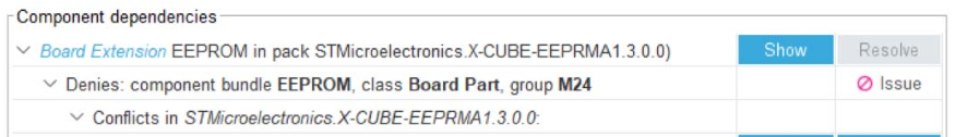
RISAF also covers the configuration of the memory sub-regions in the Memory sub-regions configuration table. Each regions have two dedicated sub-regions (see Figure 168).
Subregions are not accessible by default (grayed). To activate a given subregion, activate the related filtering parameter in the Memory regions configuration table (see Figure 169).
Memory sub-regions configuration table contains the following columns:
• RISAF region ID
• SubRegion name
• Start Address Offset and Region size: this value must be within a specific range for each region. If the user sets an incorrect value, a popup appears indicating that the value is out of range.
• SubRegion CID: values range from 1 to 7.
• Filtering
• Delegated CID
• Delegation enabled
• Read
• Write
• Secure
• Privilege
• Lock
Figure 168. Sub-regions activation in RISAF (showing activated subregions)

4.7.12 RIF code generation
The RIF configuration code generation is handled by the STM32CubeMX, which incorporates it into the initialization code of the project. The format of the generated code depends upon the type of driver used to manage the RIF. The options include HAL (Hardware Abstraction Layer) code for the Cube driver and dts-v1 (Device Tree Source version 1) code for the OpenSTLinux driver.
Note: Only dts-v1 code generation is supported.
In the context of the STM32MPU OpenSTLinux (OSTL), RIF configuration code is generated using the dts-v1 format.
The code generation adheres to the generic principles are outlined in Section 9.
The generated code is placed in a file named <project name>-mx-rif.dtsi, which is part of the master Secured firmware. Additionally, code relevant to the First Stage Bootloader (FSBL) firmware is generated in a file named <project name>-mx-fw-config.dts.
The specific syntax and semantic rules for the generated code are detailed in the RIF binding file. For more information, refer to the STM32MPU Wiki portal.
The next section details examples, including user interface screenshots and the corresponding generated code snippets. The procedure is straightforward: configure the RIF panels, click the GENERATE CODE button, and the code is produced in two files, with the RIF configuration landing in a file named <project name>-mx-rif.dtsi.
Figure 170. Example: RISUP configuration and generated code

Additionally, as described in Memory mapping generation (MPUs only), a partial memory mapping is generated.
4.7.13 Implementation of illegal access controller (IAC) feature on
STM32N6 series
The STM32N6 MCUs support a new feature, the illegal access controller (IAC).
The IAC manages all the interrupts, and the RIF utilizes the IAC feature to centralize the detection of any illegal access related to the RIF, which is managed by a secure application.
The Interrupts (IAC) panel is composed of two columns:
• IP: The name of the IP.
• IP IAC Activation: Enables the user to activate or deactivate the interrupt related to a given IP.

4.8 Pinout & Configuration view for STM32H7 dual-core products
Some STM32H7 products come with an Arm Cortex-M7 core, an Arm Cortex-M4 core, and three power domains.
For such products, the Pinout & Configuration view allows the user to:
• For each peripheral and middleware: assign it to one core context or both, whenever possible. in case both contexts are selected, assign an “initializer” core to indicate on which core the peripheral or middleware initialization function shall be called.
• For each peripheral: view the power domain it belongs to. • For GPIOs: assign it to a core or leave it free for other components that may require it. In this last case the GPIO initialization are performed on the same core as the component reserving it (code is generated accordingly).
For peripherals and middleware, these possibilities are offered in two different panels:
1. From the component tree panel, which lists all supported peripherals and middleware
(clicking the gear icon enables the “Show contexts” option), see Figure 173
2. From each component mode panel, opened by clicking the component name.
Figure 173. STM32H7 dual-core: peripheral and middleware context assignment

For GPIOs (see Figure 174), assignment is done through the Pinout view directly or later and automatically through its selection in the platform settings panel of a middleware.
Figure 174. STM32H7 dual-core: GPIOs context assignment

4.9 Enabling security in Pinout & Configuration view
(STM32L5 and STM32U5 series only)
The STM32L5 MCU series harnesses the security features of the Arm Cortex-M33 processor and its TrustZone for Armv8-M combined with ST security implementation.
STM32L5 MCUs support
• two levels of privilege
– unprivileged: software has limited access to system resources
– privileged: software has full access to system resources, subject to security restrictions
• two security states, Secure and Nonsecure: TrustZone security is activated when the TZEN option bit is set in the FLASH_OPTR register. Security states are orthogonal to mode and privilege, therefore, each security state supports execution in both modes and both levels of privilege.
In STM32CubeMX the choice to activate TrustZone is made at project creation (see Section 4.2). When TrustZone is enabled, STM32CubeMX Pinout & Configuration view is adjusted accordingly, with a split between secure (M33S) and nonsecure context (M33NS), and more security-related configuration options (see Figure 175).
Figure 175. Pinout & Configuration view for TrustZone-enabled projects

4.9.1 Privilege access for peripherals, GPIO EXTIs and DMA requests
Independently of TrustZone, STM32CubeMX enables privilege access:
• for each peripheral: in the GTZC configuration panel (see Section 4.9.5), as shown in Figure 176
• for each GPIO EXTI: in the GPIO configuration panel, as shown in Figure 177
• for each DMA channel: in the DMA configuration panel (see Section 4.9.4), as shown in Figure 178.
Note: When TrustZone is active, either all or none of the RCC registers can be put in privilege mode. In STM32CubeMX, this is done by selecting “Privileged-only attribute” check box from RCC mode panel (see Figure 179) . In privilege mode, all RCC registers configuration are reserved for the privilege application through the PWR_CR_PRIVEN bit, which is secured when Trustzone is activated.
Figure 177. Setting privileges for GPIO EXTIs

Figure 178. Configuring security and privilege of DMA requests

4.9.2 Secure/nonsecure context assignment for
GPIO/peripherals/middleware
STM32CubeMX allows the user
• to assign each peripheral and middleware to one of the contexts
• to assign a GPIO input or output to one of the context or to leave it free for other components that may require it. In this last case the GPIO assignment is in the same context as the component reserving it. By default all IOs are secured.
The assignment is done in different panels:
• For peripherals and middleware only: from the component tree panel when “Show contexts” option is enabled (clicking the gear icon) or from the mode panel.
• For peripherals only: from the GTZC configuration panel (peripherals only).
• For GPIOs only: from the configuration panel or from the Pinout view, through a right-click on the GPIO pin and by selecting “Pin Reservation”.
• For DMA requests: from the DMA configuration panel.
Note: RCC resources can be secured through the Clock configuration view (see Section 4.10.2).
Note: For middleware requiring a peripheral the middleware can only be assigned to the context the peripheral is already assigned to.
4.9.3 NVIC and context assignment for peripherals interrupts
When TrustZone is enabled, the interrupt controller is split into NVIC_NS for the nonsecure context and NVIC_S for the secure context. Two SysTick instances are available as well, one for each context: they are visible, respectively, under SYS_NS and SYS_S.
By default, all interrupts are secured.
Peripherals interrupts are automatically assigned to the interrupt controller relevant to the context:
• For peripherals assigned to the nonsecure context, interrupts are enabled on NVIC_NS.
• For peripherals assigned to the secure context, interrupts are enabled on NVIC_S.
4.9.4 DMA (context assignment and privilege access settings)
STM32CubeMX allows the user to set as privileged the DMA channel and in some cases, to secure the DMA channel, source and destination see Figure 180.
Figure 180. Configuring security and privilege of DMA requests

The DMA channel is set to non-privileged by default. The choice to set it as privileged is always available.
The choice to secure the DMA channel, source, and destination depends on the request characteristics.
There are four cases:
• The request is either a memory to memory transfer request or a DMA generator request: the channel is not secure by default but can be secured. The source and destination can be secured only when the channel is secure.
• The request is for a peripheral assigned to the nonsecure context: channel, source and destination cannot be secured (checkboxes are disabled) and so they are forced to the nonsecure context.
• The request is a peripheral to memory request for a peripheral assigned to the secure context: channel and source are automatically secured (checkboxes enabled, cannot be disabled), while there is a choice to secure or not the destination.
• The request is a memory to peripheral request for a peripheral assigned to the secure context: channel and destination are automatically secured (checkboxes enabled, cannot be disabled), while there is a choice to secure or not the source.
4.9.5 GTZC
To configure TrustZone system security, STM32L5 series come with a Global TrustZone ® security controller (GTZC). Refer to RM0438 “ STM32L552xx and STM32L562xx advanced Arm®-based 32-bit MCUs ” for more details.
In STM32CubeMX, for projects with TrustZone activated, GTZC is enabled by default and cannot be disabled. For projects without Trustzone active, GTZC can be enabled and gives only the possibility to set privileges.
GTZC is made up of three blocks that can be configured through STM32CubeMX using dedicated tabs in GTZC configuration panel:
• TZSC (TrustZone security controller)
– Defines which peripherals are secured and/or privileged, and controls the nonsecure area size for the watermark memory peripheral controller (MPCWM). The TZSC block informs some peripherals (such as RCC or GPIOs) about the secure status of each securable peripheral, by sharing with RCC and I/O logic.
– The privileges are set in the TrustZone ® Security Controller - Privilegeable Peripherals tab.
– The secure states are set in TrustZone ® Security Controller - Securable Peripherals tab (they match the assignment to context (M33S or M33NS) done on the Tree view or in the Mode panel).
– The MPCWM configuration is done through the TrustZone ® Security Controller Memory Protection Controller Watermark tab.
• MPCBB (block-based memory protection controller)
– Controls secure states of all blocks (256-byte pages) of the associated SRAM. It is configured through the Block-based Memory Protection Controller tab.
• TZIC (TrustZone illegal access controller)
– Gathers all illegal access events in the system and generates a secure interrupt towards NVIC. It is configured through the TrustZone ® Illegal Access Controller tab.
Figure 181. Securing peripherals from GTZC panel
On-the-fly decryption engine (OTFDEC) allows the user to decrypt on-the-fly AHB traffic based on the read request address information. When security is enabled in the product OTFDEC can be programmed only by a secure host.
Figure 182. OTFDEC secured when TrustZone is active

4.10 Clock Configuration view
STM32CubeMX Clock Configuration window (see Figure 183) provides a schematic overview of the clock paths, clock sources, dividers, and multipliers. Drop-down menus and buttons can be used to modify the actual clock tree configuration, to meet the application requirements.
Figure 183. STM32F469NIHx clock tree configuration view

Actual clock speeds are displayed and active. The used clock signals are highlighted in blue.
Out-of-range configured values are highlighted (as shown in Figure 184) to flag potential issues. A solver feature is proposed to automatically resolve such configuration issues.
Figure 184. Clock tree configuration view with errors

Reverse path is supported: just enter the required clock speed in the blue filed and STM32CubeMX attempts to reconfigure multipliers and dividers to provide the requested value. The resulting clock value can then be locked by right clicking the field to prevent modifications.
STM32CubeMX generates the corresponding initialization code:
• main.c with relevant HAL_RCC structure initializations and function calls
• stm32xxxx_hal_conf.h for oscillator frequencies and V DD values.
4.10.1 Clock tree configuration functions
External clock sources
When external clock sources are used, the user must previously enable them from the Pinout view available under the RCC peripheral.
Peripheral clock configuration options
Other paths, corresponding to clock peripherals, are grayed out. To become active, the peripheral must be properly configured in the Pinout view. This view allows the user to: • Enter a frequency value for the CPU clock (HCLK), buses or peripheral clocks
STM32CubeMX tries to propose a clock tree configuration that reaches the desired frequency while adjusting prescalers and dividers and taking into account other peripheral constraints (such as USB clock minimum value). If no solution can be found, STM32CubeMX proposes to switch to a different clock source or can even conclude that no solution matches the desired frequency.
• Lock the frequency fields for which the current value should be preserved
Right click a frequency field and select Lock to preserve the value currently assigned when STM32CubeMX searches for a new clock configuration solution.
The user can unlock the locked frequency fields when the preservation is no longer necessary.
• Select the clock source that will drive the system clock (SYSCLK) – External oscillator clock (HSE) for a user defined frequency.
– Internal oscillator clock (HSI) for the defined fixed frequency.
– Main PLL clock
• Select secondary sources (as available for the product)
– Low-speed internal (LSI) or external (LSE) clock
– I2S input clock
– Other sources
• Select prescalers, dividers and multipliers values • Enable the Clock Security system (CSS) on HSE when it is supported by the MCU
This feature is available only when the HSE clock is used as the system clock source directly or indirectly through the PLL. It allows detecting HSE failure and inform the software about it, thus allowing the MCU to perform rescue operations.
• Enable the CSS on LSE when it is supported by the MCU
This feature is available only when the LSE and LSI are enabled and after the RTC or LCD clock sources have been selected to be either LSE or LSI.
• Reset the Clock tree default settings by using the toolbar Reset button This feature reloads STM32CubeMX default clock tree configuration.
• Undo/Redo user configuration steps by using the toolbar Undo/Redo buttons • Detect and resolve configuration issues
Erroneous clock tree configurations are detected prior to code generation. Errors are highlighted in fuchsia and the Clock Configuration view is marked with a fuchsia cross (see Figure 184).
Issues can be resolved manually or automatically by clicking the Resolve Clock Issue button that is enabled only if issues have been detected. The underlying resolution process follows a specific sequence: a) Setting HSE frequency to its maximum value (optional).
b) Setting HCLK frequency then peripheral frequencies to a maximum or minimum value (optional).
c) Changing multiplexers inputs (optional).
d) Finally, iterating through multiplier/dividers values to fix the issue. The clock tree is cleared from fuchsia highlights if a solution is found, otherwise an error message is displayed.
Note: To be available from the clock tree, external clocks, I2S input clock, and master clocks must be enabled in RCC configuration in the Pinout view. This information is also available as tooltips.
The tool automatically performs the following operations:
• Adjust bus frequencies, timers, peripherals and master output clocks according to user selection of clock sources, clock frequencies and prescalers/multipliers/dividers values.
• Check the validity of user settings.
• Highlight invalid settings in fuchsia and provide tooltips to guide the user to achieve a valid configuration.
The Clock Configuration view is adjusted according to the RCC settings (configured in RCC Pinout & Configuration views) and vice versa:
• If in RCC Pinout view, the external and output clocks are enabled, they become configurable in the Clock Configuration view.
• If in RCC Configuration view, the Timer prescaler is enabled, the choice of Timer clocks multipliers is adjusted.
Conversely, the clock tree configuration may affect some RCC parameters in the configuration view:
• Flash latency: number of wait states automatically derived from V DD voltage, HCLK frequency, and power over-drive state.
• Power regulator voltage scale: automatically derived from HCLK frequency. • Power over-drive is enabled automatically according to HCLK frequency. When the power drive is enabled, the maximum possible frequency values for AHB and APB domains are increased. They are displayed in the Clock Configuration view.
The default optimal system settings that is used at startup are defined in the system_stm32f4xx.c file. This file is copied by STM32CubeMX from the STM32CubeF4 MCU package. The switch to user defined clock settings is done afterwards in the main function.
Figure 183 gives an example of Clock tree configuration for an STM32F429x MCU, and Table 9 describes the widgets that can be used to configure each clock.
Table 9. Clock configuration view widgets
|
Format |
Configuration status of the Peripheral Instance |
|
Active clock sources |
|
|
Unavailable settings are blurred or grayed out (clock sources, dividers,…) |
|
|
Gray drop down lists for prescalers, dividers, multipliers selection. |
|
|
Multiplier selection |
|
|
User defined frequency values |
|
|
Automatically derived frequency values |
|
|
User-modifiable frequency field |
|
|
Right click blue border rectangles to lock/unlock a frequency field. Lock to preserve the frequency value during clock tree configuration updates. |
4.10.2 Securing clock resources (STM32L5 series only)
When the TrustZone security is activated, the RCC is able, through the security configuration register, to prevent nonsecure access to system clock resources.
Accordingly, STM32CubeMX allows the user to configure as secure:
• system clock sources with a fixed frequency: HSI, LSI, and RC48 • system clock sources with a configurable frequency: HSE (+CSS), MSI and LSE (+CSS)
• two multiplexers: CLK48 clock multiplexer, System Clock (+MCO source) multiplexer • other system configurations: PLLSYS, PLLSAI1, PLLSAI2 phase-locked loops and AHB/APB1/APB2 bus pre-scalers
In the Clock Configuration view, these securable resources are highlighted with a key icon. Security is enabled using the Secure checkbox accessed through a right-click on the resource. Once the resource is secure, it is highlighted with a green square.
Configurable resources can be locked to prevent further configuration changes: this is done by selecting the Lock checkbox accessed through a right-click on the resource.
There is also a shortcut button to lock/unlock in one click all resources that are both securable and configurable.
When a peripheral is configured as secure, its related clock, reset, clock source and clock enable are also secure. In STM32CubeMX the peripheral is configured as secure in the Pinout & Configuration view and its clock source is automatically highlighted as secure using a green square in the Clock configuration view.
Table 10. Clock Configuration security settings
|
View |
Description |
|
Example of non-configurable system clock resource that is secured. |
|
|
Example of the system clock HSE clock source that is secured and remains open for editing: the frequency value can be changed. |
|
|
Example of the system clock HSE clock source that is secured and has been locked for editing: the frequency value cannot be modified. |
|
|
Example of the system clock multiplexer that is secured and unlocked: the clock source can be changed. |
|
|
Example of the main PLL multiplexer that is secured and locked. The clock source is HSE and cannot be changed. PLLxxM, PLLxxN, PLLxxP, PLLxxQ and PLLxxR are secured and locked for editing as well. |
Table 10. Clock Configuration security settings (continued)
|
View |
Description |
|
Example of the UART4 clock source multiplexer: the clock source is secured because the UART4 peripheral is configured as secure in the Pinout & Configuration view. It is set to PCLK1 and can be changed as the Lock checkbox is unchecked. |
|
|
Example of the UART4 clock source multiplexer: the clock source is secured because the UART4 peripheral is configured as secure in the Pinout & Configuration view. It is set to PCLK1 and can no longer be changed as Lock is on. |
|
|
Example of securing and locking the access to AHB prescaler. APB1 and APB2 prescalers are locked as well. |
|
|
Example of LSI highlighted as a securable resource using the key icon. |
|
|
Lock/Unlock All button (active only for secure and configurable resources). |
4.10.3 Recommendations
The Clock Configuration view is not the only entry for clock configuration, RCC and RTC peripherals can also be configured.
1. From the Pinout & Configuration view, go to the RCC mode panel to enable the clocks as needed: external clocks, master output clocks and Audio I2S input clock when available. Then go to the RCC configuration panel, and adjust the default settings if needed. Changes are reflected in the Clock Configuration view. The defined settings may change the settings in the RCC configuration as well (see Figure 185).
Figure 185. Clock tree configuration: enabling RTC, RCC clock source and outputs from Pinout view
2. Go to the RCC configuration in the Pinout & Configuration view. The settings defined there for advanced configurations are reflected in the Clock configuration view. The defined settings may change the settings in the RCC configuration.
Figure 186. Clock tree configuration: RCC peripheral advanced parameters
4.10.4 STM32F43x/42x power overdrive feature
STM32F42x/43x MCUs implement a power overdrive feature that allows them to work at the maximum AHB/APB bus frequencies (for example, 180 MHz for HCLK) when a sufficient VDD supply voltage is applied (for example, VDD > 2.1 V).
Table 11 lists the different parameters linked to the power overdrive feature and their availability in STM32CubeMX user interface.
Table 11. Voltage scaling versus power overdrive and HCLK frequency
|
Parameter |
STM32CubeMX panel |
Value |
|
VDD voltage |
Configuration (RCC) |
User-defined within a predefined range. Impacts power over-drive. |
|
Power regulator voltage scaling |
Automatically derived from HCLK frequency and power over-drive (see Table 12). |
|
|
Power over-drive |
This value is conditioned by HCLK and VDD values (see Table 12). It can be enabled only if VDD ≥ 2.2 V. When VDD ≥ 2.2 V it is automatically derived from HCLK, or can be configured by the user if multiple choices are possible (as an example, HCLK = 130 MHz) |
|
|
HCLK/AHB clock maximum frequency value |
Clock Configuration |
Displayed in blue to indicate the maximum possible value. For example: maximum value is 168 MHz for HCLK when power overdrive cannot be activated (when VDD ≤ 2.1 V), otherwise it is 180 MHz. |
|
APB1/APB2 clock maximum frequency value |
Displayed in blue to indicate the maximum possible value. |
Table 12 gives the relations between power-over drive mode and HCLK frequency.
Table 12. Relations between power over-drive and HCLK frequency
|
HCLK frequency range: VDD > 2.1 V required to enable power over-drive (POD) |
Corresponding voltage scaling and power over-drive (POD) |
|
≤120 MHz |
– Scale 3 – POD is disabled |
|
120 to 144 MHz |
– Scale 2 – POD can be enabled or disabled |
|
144 to 168 MHz |
– Scale 1 when POD is disabled – Scale 2 when POD is enabled |
|
168 to 180 MHz |
– POD must be enabled – Scale 1 (otherwise frequency range not supported) |
4.10.5 Clock tree glossary
Table 13. Glossary
|
Acronym |
Definition |
|
HSI |
High speed Internal oscillator: enabled after reset, lower accuracy than HSE |
|
HSE |
High speed external oscillator: requires an external clock circuit |
|
PLL |
Phase locked loop: used to multiply above clock sources |
|
LSI |
Low speed Internal clock: low power clocks usually used for watchdog timers |
Table 13. Glossary (continued)
|
Acronym |
Definition |
|
LSE |
Low speed external clock: powered by an external clock |
|
SYSCLK |
System clock |
|
HCLK |
Internal AHB clock frequency |
|
FCLK |
Cortex free running clock |
|
AHB |
Advanced high performance bus |
|
APB1 |
Low speed advanced peripheral bus |
|
APB2 |
High speed advanced peripheral bus |
4.11 Project Manager view
This view (see Figure 187) comes with three tabs:
• Project: to specify the project name, location, toolchain, and firmware version.
• Code Generation: to set code generation options, such as the location of peripheral initialization code, library copy/link options, and to select templates for customized code.
• Advanced Settings: dedicated to ordering STM32CubeMX initialization function calls.
Figure 187. Project Settings window
If the user chooses the CMake toolchain, a new field named “Default Compiler/Linker” appears, to enable the selection of the desired compiler (GCC/Starm-Clang).
Figure 188. Compiler option for CMake toolchain
The code is generated in the project folder tree shown in Figure 189.
Figure 189. Project folder
Note: Some project setting options become read-only once the project is saved. To modify these options, the project must be saved as new, using the File > Save Project as menu.
** Caution: ** STM32CubeMX uses reserved folder names. User cannot create new folder named Middlewares or Utilities inside project folder generated by STM32CubeMX, because, after code regeneration, those folders are deleted or modified.
4.11.1 Project tab
The Project tab of the Project Settings window allows configuring the following options (see Figure 187):
• Project settings:
– Project name: name used to create the project folder and the .ioc file name at a given project location
– Project location: directory where the project folder is stored.
– Application structure: select between Basic and Advanced options.
Basic structure: recommended for projects using one or no middleware. This structure consists in placing the IDE configuration folder at the same level as the sources, organized in sources and includes subfolders (see Figure 190)
Advanced structure: recommended when several middleware components are used in the project, makes the integration of middleware applications easier (see Figure 191)
– Toolchain folder location: by default, it is located in the project folder at the same level as the .ioc file.
– Toolchain/IDE: selected toolchain
– For the STM32MPUs, OpenSTLinux settings: location of generated device tree and manifest version and contents for current project (see Figure 192). These information enable the synchronization of the right SW components versions with STM32CubeMP1 for Cortex ® M and Linux, tf-a, u-boot for Cortex ® A. It is important to take them into account especially to ensure one Cube firmware
version is aligned with SW components for Cortex ® A around OpenAMP / RPM link and resource management API.
Selecting Makefile under Toolchain/IDE leads to the generation of a generic gcc-based makefile.
• Additional project settings for STM32CubeIDE toolchain:
Select the optional Generate under root checkbox to generate the toolchain project files in STM32CubeMX user project root folder or deselect it to generate them under a dedicated toolchain folder.
STM32CubeMX project generation under the root folder allows the user to benefit from the following Eclipse features:
– Optional copy of the project into the Eclipse workspace when importing a project.
– Use of source control systems such as GIT or SVN from the Eclipse workspace.
Choosing to copy the project into workspace prevents any further synchronization between changes done in Eclipse and changes done in STM32CubeMX, as there will be two different copies of the project.
• Linker settings: value of minimum heap and stack sizes to allocate for the application. The default values are 0x200 and 0x400 for heap and stack sizes, respectively. These values may need to be increased when the application uses middleware stacks.
• Firmware package selection when more than one version is available (this is the case when successive versions implement the same API and support the same MCUs). By default, the latest available version is used.
• Firmware location selection option
The default location is the location specified under the Help > Updater Settings menu.
Deselecting the Use Default Firmware Location checkbox allows the user to specify a different path for the firmware that will be used for the project (see Figure 193).
Figure 190. Selecting a basic application structure
Figure 191. Selecting an advanced application structure
Figure 193. Selecting a different firmware location
The new location must contain at least a Drivers directory containing the HAL and CMSIS drivers from the relevant STM32Cube MCU package. An error message pops up if the folders are not found (see Figure 194).
Figure 194. Firmware location selection error message
To reuse the same Drivers folder across all projects that use the same firmware location, select the Add the library files as reference from the Code generator tab (see Figure 195).
Figure 195. Recommended new firmware repository structure
** Caution: ** STM32CubeMX manages firmware updates only for this default location. Choosing another location prevents the user from benefiting from automatic updates. The user must manually copy new driver versions to its project folder.
4.11.2 Code Generator tab
The Code Generator tab allows specifying the following code generation options (see Figure 196):
• STM32Cube Firmware Library Package option
• Generated files options
• HAL settings options
• Custom code template options
STM32Cube Firmware Library Package option
The following actions are possible:
• Copy all used libraries into the project folder
STM32CubeMX copies to the user project folder the drivers libraries (HAL, CMSIS) and the middleware libraries relevant to the user configuration (such as FatFs, USB).
• Copy only the necessary library files:
STM32CubeMX copies to the user project folder only the library files relevant to the user configuration (e.g., SDIO HAL driver from the HAL library).
• Add the required library as referenced in the toolchain project configuration file
By default, the required library files are copied to the user project. Select this option for the configuration file to point to files in STM32CubeMX repository instead: the user project folder will not hold a copy of the library files but only a reference to the files in STM32CubeMX repository.
Generated files options
This area allows the user to define the following options:
• Generate peripheral initialization as a pair of .c/.h files or keep all peripheral initializations in the main.c file.
• Backup previously generated files in a backup directory The .bak extension is added to previously generated .c/.h files.
Keep user code when regenerating the C code.
This option applies only to user sections within STM32CubeMX generated files. It does not apply to the user files that might have been added manually or generated via ftl templates.
• Delete previously generated files when these files are no longer needed by the current configuration. For example, uart.c/.h file are deleted if the UART peripheral, that was enabled in previous code generation, is now disabled in current configuration.
HAL settings options
This area allows selection one HAL settings options among the following:
• Set all free pins as analog to optimize power consumption
• Enable/disable Use the Full Assert function: the Define statement in the stm32xx_hal_conf.h configuration file is commented or uncommented, respectively.
Custom code template options
To generate custom code, click the Settings button under Template Settings, to open the Template Settings window (see Figure 197).
The user is then prompted to choose a source directory to select the code templates from, and a destination directory where the corresponding code will be generated.
The default source directory points to the extra_template directory, within the installation folder, to use for storing all user defined templates. The default destination folder is located in the user project folder. STM32CubeMX then uses the selected templates to generate user custom code (see Section 6.3).
Figure 198 shows the result of the template configuration of Figure 197: a sample.h file is generated according to sample_h.ftl template definition.
4.11.3 Advanced Settings tab
This tab comes with three panels (see Figure 199):
• The Driver selector panel, to select the driver (HAL or LL) to be used when generating the initialization code of a peripheral instance.
• The Generated Function Calls panel, to choose whether the function calls must be generated or not, generated as static or not and in which order.
• The Register callback panel, to select the peripherals for which the register callback define must be generated as part of the stm32xxxx_hal_conf.h file.
As an example, when ADC is enabled in the register callback panel, STM32CubeMX generates
#define USE_HAL_ADC_REGISTER_CALLBACKS 1U
Choosing not to generate code for some peripherals or middlewares
By default, STM32CubeMX generates initialization code. This automatic generation can be disabled per peripheral or middleware in the Generate code column.
Ordering initialization function calls
By default, the generated code calls the peripheral/middleware initialization functions in the order in which peripherals and middleware have been enabled in STM32CubeMX. The user can then choose to re-order them by modifying the Rank number, using the up and down arrow buttons.
The reset button allows the user to switch back to alphabetical order.
Disabling calls to initialization functions
If the “ Not to be generated ” checkbox is checked, STM32CubeMX does not generate the call to the corresponding peripheral initialization function. It is up to the user code to do it.
Choosing between HAL and LL based code generation for a given peripheral instance
Starting from STM32CubeMX 4.17 and STM32L4 series, STM32CubeMX offers the possibility for some peripherals to generate initialization code based on Low Layer (LL) drivers instead of HAL drivers: the user can choose between LL and HAL driver in the Driver Selector section. The code is generated accordingly (see Section 6.2).
Figure 199. Advanced Settings window
Unselecting the Visibility (Static) option, as shown for MX_I2C1_init function in Figure 199, allows the generation of the function definition without the static keyword, and hence extends its visibility outside the current file (see Figure 200).
Figure 200. Generated init functions without C language “static” keyword
** Caution: ** For the STM32MPUs
By default the SystemClock_Config function is called in STM32Cube Cube firmware main() function, as the “Not generate Function call” box in Project Manager/Advanced Settings panel is not activated by default (see Figure 199).
This configuration is valid for running STM32Cube firmware in engineering (Cortex-M4 stand-alone) mode, and is not valid for running STM32Cube firmware in production mode: the “Not generate Function call” box must be checked under Project Manager/Advanced Settings panel, so that there is no call to SystemClock_Config() in the main() function.
4.12 Import Project window
4.12.1 Import Project feature for STM32MCU projects
The Import Project menu eases the porting of a previously-saved configuration to another MCU. By default the following settings are imported:
• Pinout tab: MCU pins and corresponding peripheral modes.The import fails if the same peripheral instances are not available in the target MCU.
• Clock configuration tab: clock tree parameters.
• Configuration tab: peripherals and middleware libraries initialization parameters.
• Project settings: choice of toolchain and code generation options.
To import a project, proceed as follows:
1. Select the Import project icon that appears under the File menu after starting a New Project and once an MCU has been selected.
The menu remains active as long as no user configuration settings are defined for the new project, that is just after the MCU selection. It is disabled as soon as a user action is performed on the project configuration.
2. Select File > Import Project for the dedicated Import project window to open. This window allows to specify the following options:
– The STM32CubeMX configuration file (.ioc) pathname of the project to import on top of current empty project.
– Whether to import the configuration defined in the Power Consumption Calculator tab or not.
– Whether to import the project settings defined through the Project > Settings menu: IDE selection, code generation options and advanced settings.
– Whether to import the project settings defined through the Project > Settings menu: IDE selection and code generation options.
– Whether to attempt to import the whole configuration (automatic import) or only a subset (manual import).
Automatic project import (see Figure 201)
Figure 201. Automatic project import

Manual project import
In this case, checkboxes allow the user to select manually the set of peripherals (see Figure 202). Select the Try Import option to attempt importing.
Figure 202. Manual project import

The Peripheral List indicates:
– The instances configured in the project to be imported
– The instances, if any exist for the MCU currently selected, to whom the configuration must be imported. If several instances are candidate for the import, the user must choose one.
Conflicts can occur when importing a smaller package with less pins or a lower-end MCU with less peripheral options.
Click the Try Import button to check for such conflicts: the Import Status window and the Peripheral list get refreshed to indicate errors (see Figure 203), warnings, and whether the import has been successful or not:
– Warning icons indicate that the user has selected a peripheral instance more than once, and that one of the import requests will not be performed.
– A cross sign indicates that there is a pinout conflict, and that the configuration cannot be imported as such.
The manual import can be used to refine import choices and resolve the issues raised by the import trial. Figure 204 gives an example of a successful trial, obtained by deselecting the import request for some peripherals.
The Show View function allows switching between the different configuration tabs (pinout, clock tree, peripheral configuration) to check the impact of the “Try Import” action before actual deployment on the current project (see Figure 204).
Figure 203. Import Project menu - Try Import with errors

Figure 204. Import Project menu - Successful import after adjustments

Choose OK to import with the current status or Cancel to go back to the empty project without importing.
Upon import, the Import icon is grayed while the MCU is configured, and it is no longer possible to import a non-empty configuration.
4.12.2 Import Project feature for STM32MPU projects
The pin-to-pin feature is a powerful tool for managing pin configurations across
STM32MP2x designs. It is possible to transfer a complete pinout setup from one project (source MPU) to another (target MPU). This feature is tailored for STM32MP2x products supporting the VFBGA 361 10x10 mm package (part numbers ending with ALx).
Devices must share the same third digit after “MP”: as an example if source is STM32MP211AAL3, target third digit must be 1.
The supported bidirectional pin-to-pin compatibilities (under the above conditions) are STM32MP21 ↔ STM32MP25 and STM32MP21 ↔ STM32MP23. This is because these devices are pin-to-pin compatible in both directions. They can be interchanged without modifications to the pin connections (except some particular cases).
Compatibility is strictly limited to the explicitly mentioned conversions and conditions. The boot mode must be the same between the source and target MPUs. For more check the following table.
Table 14. Pin-to-pin compatibility
|
STM32MP23/5 (source) |
STM32MP21 (target) |
|
STM32MP257xx |
NA |
|
STM32MP255xx |
STM32MP215xx |
|
STM32MP253xx |
STM32MP213xx |
|
STM32MP251xx |
STM32MP211xx |
|
STM32MP237xx |
NA |
|
STM32MP235xx |
STM32MP215xx |
|
STM32MP233xx |
STM32MP213xx |
|
STM32MP231xx |
STM32MP211xx |
The pin-to-pin compatibility is accessible through File > Import Project Menu.
Example
1. Create a new project using an STM32MP2 product supporting the pin-to-pin feature.
Figure 205. Creating an STM32MP211AAL3 project

2. Perform configuration (such as activate an IP, set its mode and parameters), and save this initial project.
3. Start a second project using an STM32MP25 or STM32MP23 product associated with the initial product (refer to the above conversions rules and to Table 14).
Figure 206. STM32MP251 MPU (compatible with STM32MP211)

4. Navigate to File > Import Project, then click Import Project.
Figure 207. Import Project window

Select the previously saved project file from your local drive and click OK.
Figure 208. Importing the STM32MP211 project

The pinout view is updated with the first project configuration, and the “Pin to pin compatibility” console appears, in case of warnings detection.
Figure 210. Pinout view after the project import

Usually IP names, signals, and modes match, but there can be some differences.
IP instances name, signals and pins
During conversion from STM32MP23/25 projects to STM32MP21 projects there can be a reduction in the IP instances. As an example, OCTOSPIM is removed, while, during conversion from STM32MP21 to STM32MP23/MP25, OCTOSPIM is set with a nonmultiplexed configuration.
|
STM32MP25 |
STM32MP23 |
STM32MP21 |
|---|---|---|
|
FDCAN1, FDCAN2, FDCAN3 |
FDCAN1, FDCAN2, FDCAN3 |
FDCAN1, FDCAN2 |
|
ADC1, 2, 3 |
ADC1, 2, 3 |
ADC1, 2 (ADC3 renamed ADC2) |
|
I2C1, 2, 3, 4, 5, 6, 7, 8 |
I2C1, 2, 3, 4, 5, 6, 7, 8 |
I2C1, 2, 3 (I2C8 renamed I2C3, removed I2C3, 4, 5, 6, 7) |
|
I3C1, 2, 3, 4 |
I3C1, 2, 3, 4 |
I3C1, 2, 3 (I3C4 renamed I3C3, removed I3C3) |
|
SPI1, 2, 3, 4, 5, 6, 7, 8 |
SPI1, 2, 3, 4, 5, 6, 7, 8 |
SPI1, 2, 3, 4, 5, 6 (removed SPI6, 7, SPI8 renamed SPI6) |
|
Timers |
Timers |
No TIM20 |
|
UART4, 5, 7, 8, 9 |
UART4, 5, 7, 8, 9 |
UART4, 5, 7 |
|
USB3DR |
USB3DR |
USB_OTG_HS |
|
PCIE |
PCIE |
|
|
UCPD1 |
UCPD1 |
|
|
DSIHOST |
DSI |
|
|
OCTOSPI1, OCTOSPI2, OCTOSPIM |
OCTOSPI1 |
|
|
LVDS |
|
|
|
ETHSW |
|
|
|
VENC |
|
|
|
VDEC |
|
|
|
GPU |
|
|
|
HASH1 |
HASH1, 2 |
|
|
OTFDEC1, 2 |
OTFDEC1 |
|
|
LPDMA1 |
|
|
|
ADF1 |
|
|
|
RNG1 |
RNG1, 2 |
When transitioning to STM32MP21, there can be a reduction in the number of accessible GPIOs and/or dedicated peripheral pins compared to the STM32MP23/25 products.
The associated signals are lost if an IP with existing signals in STM32MP25 is not found in STM32MP21. A warning appears in the Pin to pin console.
Table 16. Unavailable pins
|
STM32MP23/25 |
STM32MP21 |
|
PB0, PH6, PZ2, PB4, PI2, PZ4, PB8, PI3, PZ5, PF14, PI7, PZ6, PG6, PI9, PZ7, PH2, PI10, PZ8, PH3, PI11, PZ9 |
Not available |
|
VDDA18COMBOPHY, VDDCOMBOPHY |
|
|
COMBOPHY_TX1P, COMBOPHY_RX1P, COMBOPHY_TX1N, COMBOPHY_RX1N |
|
|
COMBOPHY_REXT |
|
|
VDDCOMBOPHYTX |
|
|
PCIE_CLKINN, PCIE_CLKOUTN |
|
|
PCIE_CLKINP, PCIE_CLKOUTP |
|
|
VDDPCIECLK |
Modes
When migrating an existing project from the STM32MP23/25 series to an STM32MP21 device and vice versa, it is essential to account for differences in their operating modes. The following figures show differences for the OCTOSPI1 and USB_OTG_HS peripherals.
Figure 211. Modes matching: OCTOSPI1, STM32MP211 to STM32MP251
Figure 213. Modes matching: USB_OTG_HS, STM32MP211 to STM32MP251, mode TXRTUNE)

Figure 214. Modes matching: USB_OTG_HS, STM32MP251 to STM32MP211, modes OVRCUR and VBUSEN)

4.13 Set unused/reset used GPIOs windows
These windows are used to configure in the same GPIO mode several pins at the same time.
To open them:
• Select Pinout > Set unused GPIOs from the STM32CubeMX menu bar.
Note: The user selects the number of GPIOs and lets STM32CubeMX choose the actual pins to be configured or reset, among the available ones.
• Select Pinout > Reset used GPIOs from the STM32CubeMX menu bar.
Depending whether the Keep Current Signals Placement option is checked or not on the toolbar, STM32CubeMX conflict solver is able to move or not the GPIO signals to other unused GPIOs:
– When Keep Current Signals Placement is off (unchecked), STM32CubeMX conflict solver can move the GPIO signals to unused pins in order to fit in another peripheral mode.
– When Keep Current Signals Placement is on (checked), GPIO signals is not moved and the number of possible peripheral modes is limited.
Refer to Figure 217 and Figure 218 and check the limitation(s) in available peripheral modes.

Figure 218. Set unused GPIO pins with Keep Current Signals Placement unchecked

4.14 Update Manager windows
Three windows can be accessed through the Help menu available from STM32CubeMX menu bar:
1. Select Help > Check for updates to open the Check Update Manager window and find out about the latest software versions available for download.
2. Select Help > Manage embedded software packages to open the Embedded Software Package Manager window and find out about the embedded software packages available for download. It also allows checking for package updates and removing previously installed software packages.
3. Select Help > Updater settings to open the Updater settings window and configure update mechanism settings (proxy settings, manual versus automatic updates, repository folder where embedded software packages are stored).
Refer to Section 3.4 for a detailed description of these windows.
4.15 Software Packs component selection window
This window can be opened by clicking Middleware and Software Packs from the
Pinout & Configuration tab, at any time when working on the project. It allows the user to
select Software Packs components for the current project. It features four panels, as shown in Figure 219:
• Filters panel
Can be hidden using the “Show/hide filters” button. It is located on the left side of the window and provides a set of criteria to filter the pack component list.
• Packs panel
Main panel, displays the list of software components per pack that can be selected.
• Component dependencies panel
Can be hidden using the “Show/hide dependencies” button. It displays dependencies, if any, for the component selected in the packs panel. It proposes solutions when any is found.
Dependencies that are not solved are highlighted with fuchsia icons.
Once the dependency is solved (by selecting a component among the solution candidates) it is highlighted with green icons.
• Details and warnings panel
Can be hidden using the “Show/hide details” button. It is located on the right hand side. It provide informations for the element selected in the Pack panel.
This element can be a pack, a bundle or a component. It offers the possibility to install a version of the pack available but not yet installed, and allows the user to migrate the current project to a newer version of the pack, raising incompatibilities that cannot be automatically resolved.

See Section 10 for more details on how to handle additional software components through STM32CubeMX CMSIS-Pack integration.
4.15.1 Introduction on software components
Arm ® Keil™ CMSIS-Pack standard defines the pack (*.pdsc) format for software components to be distributed as Software Packs. A Software pack is a zip file containing a *.pdsc description file.
STM32CubeMX parses the pack .pdsc file to extract the list of software components. This list is presented in the Packs panel.
Arm ® Keil ™ CMSIS-Pack standard defines a software component as a list of files. The component or each of the corresponding individual files can optionally refer to a condition that must resolve to true, otherwise the component or file is not applicable in the given context. These conditions are listed in the Component dependencies panel.
There are no component names. Instead, each component is uniquely identified for a given vendor pack by the combination of class name, group name and a version. Additional categories, such as sub-group and variant can be assigned. These details are listed in the Details & Warnings panel.
4.15.2 Filter panel
Click on to open the Filter panel
To filter the software component list, choose pack vendor names and software component classes or enter a text string in the search field.
The resulting software component table is collapsed. Click the left arrow to expand it and display all the components that match the filtering criteria.
Table 17. Additional software window - Filter icons
|
Icon |
Description |
|
|image211| Show only favorite packs. A pack is set as favorite in the Details and Warnings panel by clicking |
|
|
Show only selected components. Components are selected in the Packs panel through checkboxes or variant selection when several implementation choices are available for the same component. |
|
|
Show only installed packs. |image212| Enables to show or hide not yet installed packs. Not yet installed packs are distinguished with the icon |
|
|
Packs not compatible with this version are distinguished with the icon |
|
|
Show only packs compatible with the MCU used for the current project. |
|
|
Reset all filters |

4.15.3 Packs panel
By default, the Packs panel shows a collapsed view: all known packs are displayed with their name and for one given version (latest version is the default). Icons are used only to highlight the status of a pack version or of a component (see Table Packs panel icons).
Details and warnings and Component dependencies panels are used to provide detailed information.
The default view can be expanded by clicking the left arrows, revealing the next level, which can be a Bundle or a top component. The lowest level is the component level.
From this panel, clicking an icon highlighting a limitation or an action opens the relevant secondary panel (Details & Warnings or Component Dependency resolution).
Note: Some packs can have conditions on Arm ® cores or STM32 products, visible only when the selected MCU meets the criteria. For example, a pack stating the “<accept Dcore=”CortexM4”/>” condition shows up, but is grayed for MCUs without Cortex ® -M4 core.
Note: A pack may promote an API and be shown under the “exposed APIs” entry. Clicking the API
name allows to display additional information in the Details & warnings panel. Selecting the component implementing the API selects the API itself. STM32CubeMX generates the project with both the API .h definition file and the API implementation .c file.
Note: Some components, highlighted in gray in the component panel, are shown as read-only.
They are software components (HAL peripheral drivers or middleware offers) coming with
STM32Cube MCU embedded software package and are natively available in STM32CubeMX.
Table 18. Additional Software window – Packs panel columns
|
Column name |
Description |
|
Pack/Bundle/Component |
At pack level, shows the <name of the Software pack> At bundle level, shows the <Name of the Class>_<Bundle name, if any> At component level, shows the <Group name>/<Subgroup name, if any>. Class names are standardized by the Arm CMSIS standard(1) |
|
Version |
Shows the version that has been selected from a list of one or more available versions of a pack. Bundle and components can either inherit the version of the pack or have their own specific version. The version is shown in the Details and Warning panel. |
|
Selection |
Selects a component through a checkbox when only one implementation is available, or from a list if variants exist. |
1. The Arm® Keil™ CMIS-Pack website, http://www.keil.com, lists the following classes:
Data Exchange: Software components for data exchange
File System: File drive support and file system
Graphics: Graphic libraries for user interfaces
Network: Network stack using Internet protocols
RTOS: Real-time operating systems
Safety: Components for testing application software against safety standards
Security: Encryption for secure communication or storage
USB: Universal serial bus stack
Wireless: Communication stacks such as Bluetooth®, WiFi®, and ZigBee®.
Table 19. Additional Software window – Packs panel icons
|
Icon |
Description |
|
The pack has been added to the user favorite list of packs. Use the Details and Warnings panel to add/remove packs from list of favorites. |
|
|
The pack version is not compatible with this STM32CubeMX version. Solution: select a compatible version. |
Table 19. Additional Software window – Packs panel icons (continued)
|
Icon |
Description |
|
The pack version is not yet installed. Solution: go to the Details and Warnings panel to download the pack version to use it for a project. |
|
|
The component is not available for selection. Solution: download the pack this component belongs to. |
|
|
A component is selected and at least one condition remains to be solved. Select the line of the component with such icon to refresh the Component dependencies panel with the list of dependencies, status and solutions if any found. |
|
|
At least one component is selected and all conditions, if any, are met. |
|
|
Other pack versions are available to switch to. Solution: use the Details and Warnings panel to proceed with a change. |
|
|
Highlights the components natively available in STM32CubeMX for the currently selected MCU. They correspond to peripheral drivers and middleware stacks. For such components, the dependencies cannot be automatically resolved: go to the STM32CubeMX pinout view and enable the relevant peripheral instance or middleware in the mode panel. They will appear as selected (green checkbox) in the Component Selector. |
4.15.4 Component dependencies panel
The conditions are dependency rules applying to a given software component. When a component is selected, it shows with a green icon if there is no dependency to resolve, with a warning icon otherwise. Click |image214|
The panel is refreshed when selecting a component, providing details on the dependencies to solve and the available solutions, if found (see Table 20):
• click the Show button to show the component solving the dependency
• click the Select button to select the component solving the dependency
• when available, click Resolve button to automatically resolve the dependencies.
Table 20. Component dependencies panel contextual help
|
Contextual help |
Description |
|
No dependency to solve. |
|
|
Dependency to solve but issue encountered (no solution found or conflict). |
|
|
Dependency to solve and at least one solution found. |
4.15.5 Details and Warnings panel
Click on to show the panel (see Figure 221).
This panel is refreshed upon selecting a line from the Packs panel.
The following actions are possible from this panel:
• Add/remove the pack from the list of favorite packs
• Install the pack
• Access the pack documentation through links
• Migrate the project to a new pack version
To migrate a project to a new software pack version:
1. Open the project
2. Migrate to the new pack version
3. Generate the code
Known issue: performing step 2 after step 3 (migrating after code generation) leads to errors (wrong file path generation and project compilation failure). To fix such issue, the project must be saved as new, and the code must be generated again. Actions are possible in this panel, namely adding/removing the pack to/from the list of favorite packs, installing a pack, accessing pack documentation through links.
Figure 221. Details and Warnings panel
4.15.6 Updating the tree view for additional software components
Once the selection of the software components required for the application is complete (see Figure 222), click OK to refresh STM32CubeMX window: the selected component appears in the tree view under Additional Software ( Figure 223).
The current selection of additional software components appears in the tree view (see Figure 223). The software components must be enabled in the Mode panel and may be configured further if any parameter is proposed in the configuration panel. Hovering the mouse over the component name reveals contextual help with links to documentation.
Figure 222. Selection of additional software components
4.16 LPBAM Scenario & Configuration view
Starting with STM32CubeMX 6.5.0, for projects without TrustZone activated and on the STM32U575/585 product line, users can optionally create LPBAM applications using the LPBAM Scenario & Configuration view (see Figure 224).
Starting with STM32CubeMX 6.6.0, users can create LPBAM applications for projects with TrustZone activated on the STM32U575/585 product lines.
Thanks to this view it is possible to:
• add/remove LPBAM applications
• for each LPBAM application, create queues
• for each queue, create functional nodes using the LPBAM firmware API available for peripherals on the Smart Run Domain
• for each LPBAM application, configure the pinout, the clock tree, and HAL-related configurations for the peripherals on the Smart Run Domain.
For details on how to work with this view, refer to Section 18: Creating LPBAM projects.
Figure 224. LPBAM window
4.17 CAD Resources view
STM32CubeMX CAD Resources view allows the user to quickly access and download schematic symbols, PCB footprints and 3D CAD models for one or more design toolchains. It requires STM32CubeMX to be connected to the Internet.
To configure and check the Internet connection select Help > Updater settings to open STM32CubeMX updater settings window.
CAD Resources can be accessed from the MCU Selector window and from STM32CubeMX project view.
Access from MCU selector
• Open the MCU selector from STM32CubeMX homepage
• Select an MCU commercial part number (Marketing status must not be “Coming soon”)
• Select the CAD Resources tab to see the CAD resources (see Figure 225). - Use the slider to go down the panel and access the different resource views (Symbols, Footprint, and 3D models).
Note: For MCU commercial part numbers in “Coming Soon” Marketing status, there are no CAD resources available (see Figure 226).
To select the resources for download (see Figure 227)
• Select the design toolchain
• Select the CAD formats
• Accept terms and conditions
• Click to download
• Specify the download location
Figure 227. CAD Resources selection for download
Access from STM32CubeMX project view
• Open an STM32CubeMX project (the MCU must not be in “Coming Soon” Marketing status)
• Select the CAD tab from the Tools panel to access CAD Resources (see Figure 228).
Figure 228. CAD Resources in Tools panel
The Symbol view reflects the STM32CubeMX project pinout configuration and, optionally, the labeling (see Figure 229). The downloaded CAD files are aligned with the pinout configuration and optionally, with the labels as well.
Figure 229. CAD Resources for STM32CubeMX project
4.18 Boot path
STM32CubeMX introduces the possibility to configure the boot path for the STM32H5 series.
Note: STM32H56x and STM32H503 do not support cryptographic hardware accelerator (a feature needed for the ST-iROT and ST-uROT), therefore the full spectrum of boot paths is not available for these MCUs.
For details about boot path and its usage, read the wiki page available on www.st.com, and the guide located under the Utilities folder of the STM32Cube firmware package.
This section details, through examples, how to configure a boot path and generate the associated code. It includes compilation, encryption, and provisioning.
4.18.1 Available boot paths
The following tables give an overview of the different boot paths supported by STM32CubeMX, depending upon the device.
Table 21. Boot paths without TrustZone (TZEN = 0)
|
MCU |
Application |
OEM-iRoT → Application |
OEM-iRoT→ uRoT → Application |
ST-iRoT → Application |
ST-iRoT → uRoT → Application |
|
STM32H503x |
√ |
√ |
|
|
|
Table 22. Boot paths with TrustZone (TZEN = 1) (1)
|
MCU |
** S/NS application** |
OEM-iRoT → S/NS application, and OEMiRoT → S/NS application (assembled) |
ST-iRoT → S application |
ST-iRoT → uRoT S/NS application, and ST-iRoT→ S/NS application |
|
STM32H56x |
√ |
√ |
|
|
|
STM32H57x |
√ |
√ |
√ |
√ |
|
STM32H54 |
√ |
|
|
|

1. S: secure, NS: nonsecure.
Table 23. Boot paths for STM32H7RS devices (1)
|
MCU |
Application |
OEM-iRoT → application |
ST-iRoT → application |
ST-iRoT → OEM-uRoT → application |
|
STM32H7RSx |
√ |
√ |
√ |
√ |
1. S: secure, NS: nonsecure.
The following figures indicate the boot paths that STM32CubeMX can configure, and the entry points after reset.
The related user option bytes are configured automatically (through Trusted Package
Creator installed with STM32CubeMX), and programmed during the provisioning stage.
Figure 231. Boot paths for STM32H57x devices
Figure 232. Bootpath scheme for STM32H5_4M devices
Figure 235. Application boot path (OEM-iRoT)
Figure 237. Application boot path: ST-iRoT and uRoT secure/nonsecure project
Figure 238. Application boot path:
ST-iRoT and secure/nonsecure user application assembled
Figure 240. Application boot path:
(OEM-iRoT and secure/nonsecure user application assembled)
4.18.2 Creating a boot path project: an example
Prerequisites
• Hardware: Discovery board STM32H573I-DK-REVC
• Tools
– STM32CubeMX-6.8.0 or later
– Trusted Package Creator (embedded in STM32CubeMX installation folder)
– CubeFW must be installed through STM32CubeMX
– IAR Embedded Workbench ® rev 9.20.4 or later
4.18.3 How to configure an OEM-iRoT boot path
The following instructions describe how to generate an OEM immutable Root of Trust (OEM-iRoT) boot path. The procedure to generate other boot paths is similar, but the data required for the configuration can be different.
Step 1: Selecting the MCU
Figure 243. Peripheral initialization
If you click yes, there will be an error during the secure code compilation. By default, all peripherals are set as secure, and the memory allocation for the secure code (defined through the OEM-iRoT_boot application) is too small. Step 2: Project creation with OEM-iRoT boot path
For this example, enable TrustZone (TZEN = 1).
Figure 244. Boot paths for STM32H56x devices
Select the option “with TrustZone activated ?” on the popup window, as shown below.
Figure 245. Activate TrustZone
Step 3: Device and peripherals configuration
The device and its peripherals can be configured. In this example, the default configuration is kept.
Figure 246. Device and peripherals configuration
Step 4: Overall configuration
Configure the application ( Figure 247), then save the project ( Figure 248).
Figure 247. Configuring the project
Step 5: Boot path selection
The possible first stages are proposed according to selected device and project structure.
Figure 249. Boot path selection
• Select OEM-iRoT for this example
Figure 250. Select OEM-iRoT
Figure 251. First boot path stage
• All possible boot paths for the second stage are proposed according to the selected device and project structure.
• Select “Secure Application ”, it generates secure and nonsecure codes.
Figure 252. Select Secure Application
• Click on FINISH to generate the binary, RoT_Provisioning folder, and sub-folders.
Figure 253. Last boot path stage
Note: If a selected boot path is not supported, a warning message is displayed, and the “FINISH” button is grayed out.
Note: For STM32H56x and STM32H523x devices it is not possible to configure the OEM-iRoT boot path if the flash size of the current MCU is not aligned with the FLASH_SIZE entry in the map.properties file. A pop-up window (see Figure 255) is displayed.
Step 6: Authentication and encryption keys regeneration, option byte file generation
Customization of OEM-iROT configuration file (OEMiROT_Config.obk):
• The default configuration file of CubeFW can be used, but the default keys must be regenerated or replaced
• To customize the configuration file, proceed as follow:
a) Launch Trusted Package Creator and select STM32H5 (click edit in Project
Manager as indicated in Figure 254)
b) Open OBkey tab
c) The default keys can be regenerated
d) The OEMiROT_Config.obk file is generated. The modified parameters are saved in OEMiROT_Config
Figure 257. Authentication and encryption keys regeneration
• The H5-Image Gen1 and Gen2 tabs indicate the location of the image configuration files and the path of the binary input and output files. Keep the default settings.
Figure 258. Secure image configuration
Figure 259. Nonsecure image configuration
Figure 260. Generate the code
Figure 261. Code is generated
Additional directories, including the IDE environment, are created.
Figure 262. Secure and nonsecure IDE directories
The S and NS applications can be developed using the generated code skeletons.
Step 8: Code compilation
Select Project → Option → Build Actions. The links to the Trusted Package executable, and to the secure and nonsecure application xml files are filled automatically.
Figure 263. IDE post build commands
The secure code must be generated before the nonsecure one. Compile each code separately (right click on Project → Rebuild all). The secure and nonsecure signed and encrypted binaries are generated during the post build phase.
Figure 264. Trusted Package Creator output directory
The program cannot be flashed using an IDE. Use provisioning scripts found in the user environment, and double click on the provisioning.bat file ( Figure 265). During provisioning, log files are generated to inform the user about the activity. Follow the on-screen instructions ( Figure 266).
In the user environment, STM32CubeMX has generated an env.bat file, containing the information required for provisioning. Do not change this file.
A pop-up (see Figure 267) appears if you forget to compile the project OEMiRoT_Boot in the CubeFW.
4.18.4 How to configure an ST-iRoT boot path
The configuration for an ST immutable Root of Trust (ST-iRoT) boot path. The requirements are the same of the previous example. Step 1: Generating the code
• Select an STM32H57x MCU
• Create a project with TrustZone activated (TZEN = 1)
• In Project Manager, choose “Secure Project”
• Save the project
• Go to “Boot Path and Debug Authentication” tab, and press the Select button
• Choose ST immutable Root of Trust (ST-iRoT)
Figure 268. Select ST-iRoT
• Select Secure Application
• Click “FINISH”, the boot path configuration panel is displayed (see Figure 270), use it to configure the application, then press the GENERATE CODE button to generate the code for the selected toolchain
Figure 270. Boot path and Debug Authentication tab
For this boot path, only the secure project is generated.
Figure 272. Code is generated
Additional directories, including the IDE environment are created.
Figure 273. Secure project completed
Secure applications can be developed using the generated code skeletons.
The Post build command creates a secure compiled encrypted code for the provisioning.
Step 2: Code compilation
The generated binaries are automatically encrypted
• Open the project in the selected toolchain, for example IAR
– Select: Project → Option → Build Actions
– The links to the Trusted Package executable and to the secure application xml are filled automatically
– Compile secure (right click on Project → Rebuild all)
Figure 274. IDE post build commands
ST-iRoT board provisioning
The program cannot be flashed using an IDE, use the provisioning scripts found in the user environment.
• Double click on the provisioning.bat file ( Figure 275)
Figure 275. Board provisioning
• During provisioning, log files are generated to inform the user about the activity
• Follow the on-screen instructions ( Figure 276)
Figure 276. On-screen instructions
In the user environment STM32CubeMX has generated an env.bat file containing the required data for provisioning, do not change it.
Figure 277. Environment configuration file
4.18.5 How to configure an assembled boot path
The configuration described below is an example of an assembled boot path.
Prerequisites:
• Hardware: Discovery board STM32H573I-DK-REVC or later
• Required tools
– Secure manager package, to be downloaded and installed from www.st.com – STM32CubeMX-6.9.0 or later
– STM32 Trusted Package Creator (embedded in STM32CubeMX installation
folder)
– IAR Embedded Workbench rev 9.20.4 or later, and the patch in the
STM32CubeH5 firmware (Version 1.1.0 or later), named EWARM/EWARMv8_STM32H5xx_Vx.x.x.zip.
Step 1: Configure flash_layout.h file
• Go to STM32Cube\Repository\STM32Cube_FW_H5_VX.X.X\Projects\ STM32H573I-DK\Applications\ROT\OEMiROT_Boot\Inc
• Open flash_layout.h
• Set the value of this define to 1 to assemble the secure and nonsecure binaries into one: #define MCUBOOT_APP_IMAGE_NUMBER 1.
Figure 278. The flash_layout.h file
Step 2: Compile OEMiROT_Boot project - Open OEMiROT_Boot with your preferred tool chain, and recompile the project.
– The map.properties file is automatically updated
(CODE_IMAGE_ASSEMBLY=0x01)
– The image file (OEMiRoT_NS_Code_Image.xml) is automatically updated (firmware area size)
Step 3: OEMiROT (assembled) code generation
• Open STM32CubeMX application and create a new project with the H5 series
(example: choose “STM32H573ZITxQ”)
• Go to Project Manager window, and select secure and nonsecure application
• Add a name for the project and save it
• Go to Boot Path and Debug Authentication Panel: in Boot path selection, click on Select button
• Select OEM-iRoT in the boot path wizard window, and click Next
• Select Secure application, and click Finish
Figure 279. The map.properties file
• Generate and build the project
• Open the project folder. A Python script assembles both binaries (Secure, Non Secure), then the TPC signs them:
– Assembled_OEMiRot_Boot_Path_Example_assembled.bin → File assembled by the Python script
– Assembled_OEMiRot_Boot_Path_Example_enc_sign.hex → File signed by the TPC
Figure 283. Project folder
• The post build command is added only for the Non Secure project.
4.18.6 How to configure OEM-uRoT (STiRot uROT) boot path
• Select an STM32H57x MCU
• Create a project with TrustZone activated (TZEN = 1), see Figure 284
• In Project Manager, save the project, see Figure 285 • Go to “Boot Path and Debug Authentication” tab, and press the Select button, see Figure 286
• Select “ST immutable Root of Trust (ST-iRot)”, then click “NEXT”, see Figure 287
• Select “OEM updatable Root of Trust (OEM-uRoT)”, then click “NEXT”, see Figure 287
• Select “Secure Application”, then click “FINISH”, see Figure 288 • The panel of boot path configuration is displayed, use it to configure the boot path in the “Boot Path and Debug Authentication” tab, see Figure 289
• Generate and build the project, see Figure 292 and Figure 293
4.18.7 How to configure ST-iRoT boot path with STM32H7RS devices
Go through the following steps:
1. Select an STM32H7S3Vx MCU ( Figure 294)
2. A popup (see Figure 295) asks to preconfigure the Memory Protection Unit. It is recommended to optimize the speculative read access of the core. Select “Yes” to keep the default configuration.
3. In Project Manager Window, check only “Appli Project”, name the project, and save it ( Figure 296).
Go to “Boot Path and Debug Authentication” tab and press the Select button ( Figure 297). 5. Select “ST immutable Root of Trust (ST-iRoT)”, then click “NEXT” ( Figure 298).
6. Select “Application”, then click “FINISH” ( Figure 299).
7. The panel of boot path configuration is displayed (see Figure 300), use it to configure the boot path in the “Boot Path and Debug Authentication” tab.
|
|
|
Figure 298. First boot path stage

Figure 300. Boot path and debug authentication panel

Note: For STM32H5 devices with a 4-Mbyte flash size, the Boot Path feature is only supported in TrustZone-enabled projects. Its configuration is no longer performed in the STM32CubeMX user interface.
In the STM32CubeMX user interface, links are provided to wiki pages for each supported Boot Path type. These pages guide the user on how to configure the Boot Path both before and during the provisioning stage.
Figure 303. The supported Boot Path in STM32H5 with 4-Mbyte devices

4.19 HSP middleware “HSP_Engine”
4.19.1 Outline of HSP
The hardware signal processor (HSP) is an on-chip hardware accelerator that is used to compute intensive signal-processing tasks instead of the CPU.
Using the HSP improves real-time performance and reduces CPU load. It is intended for:
• Running real-time control loops
• Performing metering and measurement calculations
• Processing small convolutional neural networks
• Handling general signal-processing tasks
The main component of the HSP is a high-performance signal processor engine (SPE). It supports computations in both 32 bit floating-point and 8 bit integer formats, and is responsible for running the HSP microcode, or firmware.
4.19.2 STM32CubeMX implementation for HSP
STM32CubeMX enables the configuration of:
• The HSP features - including middleware parameters and modes
• Peripheral settings
• Clock tree
• GPIO pins.
It automatically generates the code required to run applications that make use of the HSP.
The implementation of this feature is divided into two parts at STM32CubeMX level:
• HSP peripheral [HSP1]
• HSP Middleware [HSP_ENGINE]
HSP peripheral [HSP1]
The HSP configuration screen is illustrated in the following figure.
Figure 304. HSP1 Modes and configuration in STM32CubeMX

HSP1 supports the following two modes:
– The Activation mode without parameters
– The Debug mode
The activation of these modes is illustrated in Figure 305: Activating the debug mode for the HSP1 peripheral.
Figure 305. Activating the debug mode for the HSP1 peripheral

The interruptions are managed in the IP, through the NVIC settings tab as illustrated in the figure below.
Figure 306. NVIC interrupt table for the HSP1 peripheral

– HAL drivers are copied into the project directory.
– Once HSP1 IP is enabled the corresponding HSP_Engine middleware is enabled automatically.
– MX_HSP_Engine_Init method is called in main.c and its implementation is in hsp_engine.c.
HSP Middleware [HSP_ENGINE]
• The HSP_ENGINE is used by the application to run one of the following tasks:
– DSP
– CNN
– direct
– processing list.
• It supports two modes:
– Accelerator mode
– Sequencer mode
Accelerator mode
– The Accelerator mode allows users to configure parameters listed under the general tab once the “Accelerator” option is checked in the mode.
– The configurations by STM32CubeMX are illustrated in the screenshot listed below.
The following figures illustrate the activation of HSP_Engine in Accelerator mode:
Figure 307. Activating the HSP in Accelerator mode

Figure 308. Parameters to be configured for HSP feature in the Accelerator mode

The following figures illustrated the configuration of HSP_Engine in Accelerator mode:
Figure 310. Parameters to be configured for HSP feature in the Accelerator mode

Figure 312. Clock configuration view for HSP in Accelerator mode

The following figures illustrate the steps before code generation:
Figure 313. Code generation for HSP in Accelerator mode

Figure 314. Files copied from firmware while generating the code

Sequencer mode
The Sequencer mode is implemented in STM32CubeMX UI via tabs under the configuration section as described below.
• General tab
The “General tab” contains:
– General settings of the middleware.
– Settings of the modules to be integrated.
– Clock settings.
The parameters in this tab may relate either to the Sequencer or to the Accelerator mode. The tab is illustrated in the figure below.
Figure 316. General tab

• Processing List tab
The Processing List tab is illustrated in the figure below.
Figure 317. The processing list tab

A portion of the microcode (firmware) is stored in a dedicated private ROM and provides optimized signal processing routines, referred to as processing functions.
The HSP is capable of executing ordered sequences of these operations, called processing lists.
A given processing list is characterized by its name:
– The processing list name must be unique since it distinguishes one processing list from another.
– The UseEvent parameter is represented as a checkbox. When this checkbox is selected, an additional GUI section appears, allowing the configuration of the associated event such as source, type, synchronization, and so on.
Figure 318. A processing list associated with an event

Actions that can be performed on a processing list:
– Add list: Creates a new list.
– Add function: Insertse functions into the created lists.
– Delete: Clears the whole processing list.
– Show snippet code: Displays the appearance of the generated code.
Figure 319. Snippet code action
– The elements of a processing list are functions.
– A given function is characterized by:
A function.
An argument which is a list that changes depending on the chosen function.
Figure 320. Function category
• Buffers tab
The buffer tab groups the following items:
– The argument parameter depends on other HSP GUI elements, which are buffers found under the Buffers tab.
– BRAM provides the memory space that holds the data used by the processing list and the created buffers.
– The processing list uses buffers to read/write data from/to BRAM.
This is illustrated in the figure below.
Figure 321. Buffers tab
• State Buffers tab
A state buffer is used whenever an algorithm needs to preserve internal information between successive processing calls.
The UI allows the declaration of state buffer resources in HSP BRAM memory space. These kinds of resources are required for “FIR & IIR” processing functions used by the processing list.
Figure 322. State buffers tab
• Events tab
The processing list tab is linked with another tab which is the events one.
The events tab lists the used events that are generated during the execution of that list and how they are handled.
Note: A used event is an event associated with a processing list through the combo box ID, with the box “UseEvent” checked.
Only events with ID in the range [1, 22] can be used and configured, Event IDs outside this range can be associated to a processing list but cannot be used or configured since the checkbox “UseEvent” is unchecked and grayed out.
The Event tab is a read only tab. It displays only the events linked to the processing list.
Figure 323. A processing list linked with an event
Figure 324. Events tab
• Output Triggers tabs
The output trigger is a signal generated by the HSP (or by the processing list logic) to indicate that a specific event related to the processing list has occurred. This is illustrated in the figure below.
Figure 325. Output Triggers tab
When the Trigger Output is enabled and the source for a given trigger is selected from the dropdown list, the corresponding code is automatically appended to the end of the hsp_engine.c file in the generated project.
** /* Configure the Trigger Output */ if (HSP_CORE_OUTPUT_SetConfig(&hmw, HSP_CORE_TRGO_0, HSP_CORE_TRGO_SRC_STREAM) != HSP_CORE_OK)**
** {**
** Error_Handler();**
** } if (HSP_CORE_OUTPUT_Enable(&hmw) != HSP_CORE_OK)**
** { **
** Error_Handler();}**
• The code generation
For Accelerator mode:
The section below lists the generated code for an STM32CubeMX project that configures HSP_ENGINE middleware in Accelerator mode.
Figure 326. Generated Project tree for HSP configured in Accelerator mode

a-1) Under HSP_Engine/App folder:
The app_hsp_bram_alloc.c file contains the instructions for memory allocation of
BRAM
The app_hsp_engine_process.c file contains the declaration and initialization of the middleware, located in the App folder for the HSP_Engine. a-2) Under HSP_Engine/Target folder:
The hsp_engine.c implements the function that initializes the low-level portion of the driver, HSP_Engine_IF_Init(). It also implements the functions that enable and disable the peripheral clock, HAL_HSP_MspInit() and HAL_HSP_MspDeInit().
For Sequencer mode:
The section below lists the generated code for an STM32CubeMX project that configures HSP_ENGINE middleware to treat two processing lists:
– ProcessingListExample1
– ProcessingListExample2
The project tree for the HSP configured in Sequencer mode:
Figure 327. Generated Project tree for HSP configured in sequencer mode

In the main.c file located in the User/core directory, the MX_HSP_Engine_Init() and MX_HSP_Engine_Process() functions are called. Generated files for HSP configured in Sequencer mode: b-1) Under HSP_Engine/App folder:
The app_hsp_bram_alloc.c file: generated file to implement all memory allocation in BRAM
The app_hsp_engine_process.c file: generated template file that allows the user to implement his own process functions for example Run Direct, DSP, CNN commands Run Processing with CDEG or CSEG interfaces app_hsp_engine_seq.c file:
This file contains the definitions of the functions listed below (the logic for the record and configuration of Processing lists):
– MX_HSP_SEQ_Record_PL_ProcessingListExample1()
– MX_HSP_SEQ_Record_PL_ProcessingListExample2()
The hsp_engine.c contains instructions to perform the following steps:
1) Enabling HSP event generation
2) Allocating BRAM resources
3) Handling the processing list (calling the recording PL functions)
4) Configuring the trigger output
Note: For the both Accelerator and Sequencer modes, the content for files under Drivers and Middlewares folder are copied from the firmware into the project tree.
4.20 PLAY feature presentation
4.20.1 Introduction
The PLAY IP is a programmable logic array integrated into STM32 devices to allow users to create custom logic and state machines directly within the MCU, without the need for external programmable logic devices like FPGAs. This document describes how to manage and configure the PLAY IP in STM32CubeMX, specifically for the STM32H5 4M series.
4.20.2 Peripheral overview
PLAY is a flexible logic array composed of programmable logic elements (look-up tables, LUTs) with four inputs and one output each. It supports complex logic functions by cascading these elements. Inputs and outputs can be selected from external GPIOs, internal peripheral signals, or software registers.
Figure 328. PLAY feature in STM32CubeMX

Activation and mode selection
Activate the PLAY feature by selecting the checkbox located in the Mode tab of the user interface.
When the “Activated” option is selected, two groups of parameters (two main modes) are accessible in the Mode section:
• Inputs activated: A list of 16 check-boxes, each representing a GPIO signal required for the operation of the PLAY IP, is named PLAY_IN. - Outputs activated: A list of 16 check-boxes, each representing a GPIO signal generated by the PLAY IP, is named PLAY_OUT.
Each group corresponds to a tab in the Configuration part:
• Input MUX settings: 16 independent multiplexers each dedicated for configuring a specific input. - Output MUX settings: 16 independent multiplexers each dedicated for configuring a specific output.
Figure 329. Activating the PLAY feature
4.20.3 Key features
16 inputs
Sixteen inputs are selectable from a maximum of 128 signals. The system implements 16 independent multiplexers (MUXs), each supporting eight input signals. One input per MUX is sourced from a GPIO signal, which must be activated at the beginning.
• The 128 signals include 16 external GPIOs and internal signals from peripherals such as TIM, SAI, MDF, or clocks such as LSE, HSI.
Figure 330. Input Signals
For each selected input, the user can perform the following actions:
• Change the signal names to simplify the configuration. By default, the system uses the name of the signal.
• Set the minimum pulse width. Configure the filtering mode by specifying the minimum pulse width. The mode can be set to bypass (default) or to a value from 1 to 255. • Set the edge detection by defining the kind of edge transition (rising, falling or both). The Bypass option is used to disable the mode which is the default option.
Start by selecting the source for MUX n. After a signal is chosen, the system automatically displays options for the user name, minimum pulse width, and edge detection settings.
Figure 331. Input settings to be filled by the user

16 Outputs
Sixteen discrete MUX units are implemented. Each MUX acts as a 32-to-1 selector, providing access to a pool of 16 immediate LUT outputs and 16 clock-stabilized registered outputs.
An output can be direct or registered with clock-enable options.
Figure 332. Setting the Output Source for the MUX0 from the list of outputs
Figure 333. Output settings
Feedback of registered outputs to inputs enables finite state machine creation.
Logic elements
Configure the logic elements by using the “Look Up Table Settings” tab in the STM32CubeMX user interface.
• The “Look Up Table Settings” tab contains 16 groups of settings.
• Each group of settings is named LookUp Table X (where X can be a value from 0 to 15) and has the following parameters:
– Input0
– Input1
– Input2
– Input3
– LUT truth table
– Clock gate
Figure 334. Entries for the Look Up table
Input X:
Once an input X is enabled, the following parameters are added to the GUI:
– Signal Type X – Signal Name X
• Signal Type X:
A drop down list used to select the input category.
The available categories are:
– Output of IN MUX
– SW Trigger
– LUT direct output signal – LUT registered output signal
• Signal Name X:
A dependent field where the content is determined by the value selected in Signal Type X.
After a type is chosen, this field presents the list of all valid signals for that category and allows the user to select one of them (The list depends of Input Category).
For Output Registered Signals a warning should be displayed if the corresponding Clock Enable Parameter is Off.
For Input Signals, the list of User Names should be displayed and grayed out if not enabled from I/Os Activated Mode or if the peripheral is deactivated.
By default, the value is set to SWIN 15.
LUT Truth table
Figure 335. LUT truth table parameter

The LUT truth table consists of two elements:
• Field 1: A field that displays the result of the calculation performed on the input, depending on the output required by the user in the “OUT column”.
• Field 2: A grid icon that, when selected, opens the visual representation of the LUT truth table.
This is a dynamic visual representation. If the user enables any input, the system adds rows and populates them with the already configured input.
To obtain the result, which is a compact representation of how OUT behaves for all possible input combinations, the user must select the “OK” button.’
Figure 336. LUT Calculation table
Clock gate:
A graphical user interface parameter that indicates whether the clock toggles the flip-flop (normal operation), or not.
Figure 337. LUT calculation table example
When some inputs are disabled in the “Logic Element Settings”, the table is simplified. All inputs remain visible, but unused ones are marked with “x”.
In the previous representation in[3] and in[1] are enabled, in[2] and in[4] are disabled.
In the next representation all the inputs are enabled.
Figure 338. LUT inputs enabled

• Inputs: Up to 16 inputs are selectable from GPIOs and internal signals, each input can be customized and synchronized.
• Outputs: PLAY GPIOs are selectable as outputs, with options for registered or direct output.
• The signal interconnect matrix is product-specific and unique to each STM32 derivative.
• Only one GPIO input per PLAY input is permitted.
4.20.5 Configuration in STM32CubeMX
The PLAY IP can be enabled by selecting the checkbox in the Logic Array section.
Configure inputs and outputs are configured in the Pinout & Configuration tab.
Input settings include custom naming, minimum pulse width (bypass or 1-255), edge detection mode, and input source selection from the interconnect matrix.
Logic element settings allow the selection of inputs by category, such as input multiplexer outputs, software inputs, and output signals.
LUT values can be edited directly or via a popup helper.
Output MUX settings allow the selection of output sources (direct or registered), with a default disabled state.
NVIC settings allow the configuration of PLAY interrupt events.
STM32CubeMX validates configurations, for example, warns if a flag transition is set without kernel clock enabled.
4.20.6 Functional description
The PLAY logic array processes input signals by programmable LUTs to generate outputs.
Inputs can be filtered to ignore pulses shorter than a configured minimum width or to detect specific edge transitions.
Registered outputs are clocked by selectable clocks, to enable synchronous logic and state machines.
Outputs can generate flags. These flage can trigger interrupts handled by the processor.
Feedback loops enable complex finite state machine implementations.
The configuration interface in STM32CubeMX provides intuitive control over all parameters, to ensure valid setups.
4.20.7 Typical use cases
Custom logic implementation within STM32 MCUs without external FPGA/PLD.
Finite state machines for control applications.
Signal conditioning and filtering for asynchronous inputs.
Interrupt generation based on complex input conditions.
Embedded logic for industrial, automotive, or IoT applications that require low-latency logic.
4.20.8 Software and middleware support
PLAY configuration is generated by STM32CubeMX as initialization code (HAL and LL layers).
Arrays for input MUX, LUT settings, and output MUX are created in MX_PLAY1_Init function.
Disabled sources are not generated in code.
HAL and LL drivers support the configuration of inputs, LUTs, and outputs.
STM32CubeMX generates code that is consistent with the configured parameters. The generated code includes synchronization and interrupt setup.
4.20.9 Example configuration and code snippet
Input mux settings
Configure inputs from GPIO and internal signals. The INPUT0 is configured in the example below.
Set the minimum pulse width and edge detection for filtering.
LUT Settings (Look Up Table 0 is configured in the example) Enable inputs used in LUT calculation.
Use the pop-up window to calculate LUT truth table values.
Output mux Settings
Select output source as direct or registered signal.
Enable clock for registered outputs if filtering is used.
Code snippet generated by CubeMX (simplified):
/**
* @brief PLAY1 Initialization Function
* @param None
* @retval None
** */ static void MX_PLAY1_Init(void)**
{
** /* USER CODE BEGIN PLAY1_Init 0 */**
** /* USER CODE END PLAY1_Init 0 */**
** HAL_PLAY_IN_ConfTypeDef configINPUTs[CONFIGURED_INPUT_NBR]; HAL_PLAY_LUT_ConfTypeDef configLUTs[CONFIGURED_LUT_NBR];**
** HAL_PLAY_OUT_ConfTypeDef configOUTPUTs[CONFIGURED_OUTPUT_NBR];**
** /* USER CODE BEGIN PLAY1_Init 1 */**
** /* USER CODE END PLAY1_Init 1 */**
** hplay1.instance = PLAY1;**
** if (HAL_PLAY_Init(&hplay1) != HAL_OK)**
** {**
** Error_Handler();**
** }**
** /** Configure Input 0**
** */ configINPUTs[0].min_pulse_width = 0; configINPUTs[0].mode = HAL_PLAY_EDGE_DETECTION_BYPASSED; configINPUTs[0].source = HAL_PLAY1_IN_TIM3_TRGO_MUX0;**
** if (HAL_PLAY_INPUT_SetConfig(&hplay1, configINPUTs, CONFIGURED_INPUT_NBR) != HAL_OK)**
** {**
** Error_Handler();**
** }**
** /** Configure the Logic Element 0**
** */ configLUTs[0].lut = HAL_PLAY_LUT0; configLUTs[0].truth_table = 0x88;**
** configLUTs[0].input_source[HAL_PLAY_LUT_INPUT0] = HAL_PLAY_LUT_INPUT_SWTRIG15;**
** configLUTs[0].input_source[HAL_PLAY_LUT_INPUT1] = HAL_PLAY_LUT_INPUT_SWTRIG15;**
** configLUTs[0].input_source[HAL_PLAY_LUT_INPUT2] = HAL_PLAY_LUT_INPUT_LUT0_OUT_DIRECT;**
** configLUTs[0].input_source[HAL_PLAY_LUT_INPUT3] = HAL_PLAY_LUT_INPUT_SWTRIG15; configLUTs[0].clk_gate_source = HAL_PLAY_LUT_CLK_GATE_OFF;**
** if (HAL_PLAY_LUT_SetConfig(&hplay1, configLUTs, CONFIGURED_LUT_NBR) != HAL_OK)**
** {**
** Error_Handler();**
** }**
** /** Configure Output 0**
** */ configOUTPUTs[0].output_mux = HAL_PLAY_OUT0; configOUTPUTs[0].lut_output = HAL_PLAY_LUT1_OUT_REGISTERED;**
** if (HAL_PLAY_OUTPUT_SetConfig(&hplay1, configOUTPUTs, CONFIGURED_OUTPUT_NBR) != HAL_OK)**
** {**
** Error_Handler();**
** }**
** /* USER CODE BEGIN PLAY1_Init 2 */**
** /* USER CODE END PLAY1_Init 2 */**
}
4.21 Notification Service
4.21.1 Introduction
The Notification Service in STM32CubeMX allows users to subscribe to notifications, updates, or premium content when downloading or installing STM32 software.
The objective is to obtain user consent to allow ongoing communication related to STM32 software, such as new releases and documentation updates.
Behavior overview:
• The Notification Service window in STM32CubeMX is accessible via a tab named Notification Service under the help menu, then Connection & Updates option.
Figure 339. Notification Service window in STM32CubeMX

• A subscription proposal for the software is triggered if the user tries to download or install it (If there is no existing notification subscription).
Figure 340. Popup appearing while installing a package for non-registered users
The Notification Service prompts the user to subscribe at the following entry points:
• When downloading an STM32Cube firmware package.
• When generating code.
• In the “Project Manager Settings” dialog.
• In the “Check for Update” window.
• In the Example Selector.
• In the Bootpath configuration.
• In the Third Parties window.
• In the “Connection & Updates” window.
The subscription proposal appears at each download attempt until the user selects “Don’t ask me again”.
Choosing “Don’t ask me again” automatically checks the “Hide notification service subscription prompt” box under the Notification Service window.
Figure 341. Hiding notification service prompt
Figure 342. Subscription proposal appearing while installing firmware
Users who want to subscribe must click the ‘Register’ button in the Notification Service window. This opens a registration form that must be completed to access the ‘Subscribe’ button. Once subscribed, users can:
• View their notification subscription status, including the current email address used.
• Update the notification subscription (change the email address).
• Clear the email address (see details below).
4.21.2 Subscription / Unsubscription
Subscription
To subscribe, the user must complete the registration form for the notification service.
• Subscription form elements:
– Email (mandatory):
The user provides an email address.
The form implements basic formatting validation to check the email syntax.
– Company (optional):
The user may provide a company name.
– Link to privacy notice:
The form includes a link to the ST standard corporate privacy policy.
– Checkbox to keep local history (if any exists):
Select this option to retain and associate previous local download history with the new subscription.
Figure 343. Register form
Subscription requirements
• A valid and operational email address.
• The user must have access to the email inbox used for the subscription.
The subscription starts only after the user validates the email address by clicking on the verification link sent to the inbox.
Figure 344. Popup for email validation
Figure 345. Email validation
• After the user selects the Validate now button in the received email, the browser redirects the user to an ST web page that displays the subscription details.
Figure 346. ST Web page to validate the subscription
This process prevents users from subscribing using someone else’s email address.
Note: Subscription to the Notification Service does not require any account creation on st.com.
Figure 347. The view of Notification Service tab after a user subscription

Subscription flow
• When the end-user subscribes to the Notification Service:
– The user’s credentials are saved under the user’s home folder.
– Each subsequent software download from STM32CubeMX (Software download history) is included in the user’s preferences and notification.
– Prior to email verification, the STM32CubeMX generates a local file to save the user’s preferences.
– When the user validates the email, the local history is removed from the user’s machine.
– The download history is displayed on the subscription page “My Subscriptions - STMicroelectronics” (the user should log with an account).
Figure 348. The subscription page
• The user can handle the preferences in the following page “My Communication preferences - STMicroelectronics”

• STM32CubeMX exposes the subscribed email address in its UI so that the user can:
– Update it to fix a typo, or change email for example.
– Clear it (see next section).
Figure 351. The user name exposed in the Notification Service window after email validation
4.21.3 Clearing the email in STM32CubeMX
If the user clears the email address in STM32CubeMX:
STM32CubeMX stops sending the software download history to the backend database. • The user’s existing subscription to notifications is not automatically canceled. Notifications may continue according to the configuration stored on the server side (preferences center / st.com).
Clearing the email in STM32CubeMX is a local application action and is not necessarily propagated as an unsubscription to the backend database.
4.21.4 Unsubscription
Unsubscription from notifications occurs through links provided in notification emails.
Each notification email will contain:
• A direct link to an unsubscribe page.
• A link to the Preference Center (under login on st.com), where the user can manage all the preferences and notifications.
The Preference Center is responsible for the actual activation/deactivation of email notifications.
Figure 354. The unsubscription action
4.21.5 Notification logic of firmware and software preferences
Start of notifications
After successful email validation, notification sending starts. The user must click the link sent to the inbox to validate the email address.
Frequency
Notifications are sent on a weekly basis at most.
A weekly email is sent only if there are changes relevant to the user’s preferences.
Notification content
Each notification email may include:
• New versions of preferred STM32 software such as STM32Cube firmware packages and so on.
• New versions of technical documents associated with the user’s software preferences.
• A link to the product folder on st.com
– This implies that the new software version is published on st.com.
• A summary of the user preferences (software and other preferences).
The email explicitly mentions that the software can be downloaded directly inside
STM32CubeMX.
Links in notification Email
At the bottom of the notification email, there are two links:
1. Unsubscribe
Stop the notification subscription according to backend rules.
2. My preference center
A link to the full preference center on st.com (under login).
The user can manage and update:
– All subscriptions,
– All notification channels,
– All software and other preferences.
4.22 About window
This window displays STM32CubeMX version information. To open it, select Help > About from the STM32CubeMX menu bar.
Figure 355. About window