
5 STM32CubeMX tools 
5.1 External Tools 
This panel is accessible from the home page. It provides an overview of the tools relevant for the STM32 product portfolio (see Figure 356):
5.2 Compare Projects 
This new feature is designed to enable the comparison of two projects, based on the same or on different microcontrollers. This tool allows users to efficiently analyze and correlate similarities and differences in IP configurations and project structure between two projects.
5.2.1 User interface of the Compare Projects tool 
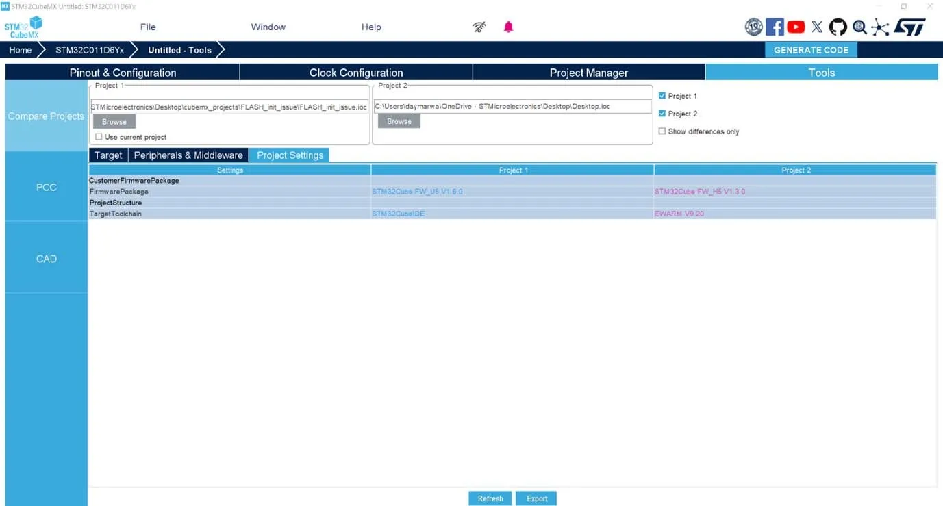
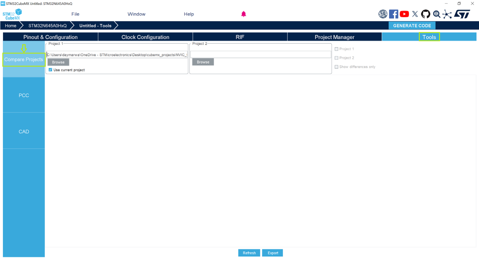
The user can activate this function from the Tools panel by clicking the Compare Projects field (see Figure 357), or from the home page (see Figure 358) by clicking ACCESS TO COMPARE PROJECT under Other services (even before creating any project).
Figure 357. Reaching Compare Project from the Tools panel
Two main panels, named Project 1 and Project 2.
Each field contains a “Browse” button from where we can load the desired .ioc file.
The check box “Use Current project” in the first panel is to use the opened project in STM32CubeMX instead of loading a saved one in the local device.
Three check boxes, named Project 1, Project 2, and “Show differences only”:
Once the second project is loaded, the Project 1 and Project 2 check boxes are checked systematically, indicating that the output table contains all the parameters of Project 1 and Project 2 (whether they are different or not).
If the user wants to see only the parameters that are different between the two projects, it can check “Show differences only”.
Refresh button: once clicked, it performs an instantiated comparison. • Export button: allows users to save or transfer the result of the comparison to an external file in Excel format.
Figure 359. User interface of the Compare Projects tool
Load the first project from the local device (Figure 360).
Once the first .ioc is loaded, a popup appears to indicate the need to upload the second .ioc.
Load the second project (Figure 361).
After uploading the second .ioc file, the output is displayed in the UI (Figure 362).
If the user uploads the same .ioc file (having the same path) into the two fields, a popup appears to indicate that it is irrelevant to perform a comparison (Figure 363).
If the two projects have the same structure and the user checks “Show differences only”, only the headers of the respective tables “Target”, “Peripherals & Middleware”, and “Project Settings” are shown, no data are displayed (Figure 364).
Load a project from local and start comparing it as the current project (Project 1).
Compare a newly created project (after configuration), even unsaved, with a saved project, see Figure 365.
Compare a currently open project with itself (the popup blocking the comparison of two similar projects does not appear), see Figure 366:
Load a the first project saved on the local as the current project (current project automatically ticked and the configuration can be modified after loading)
Load the same project file from the local in the Project 2 field.
Figure 365. Compare the current non saved project with another project 
5.2.3 The output of the comparison 
After starting the comparison, the following elements are added to the UI:
Target table ( Figure 367): provides a comparison of the parameters used in each project. It clearly shows differences in:
Part numbers
Number of IOs
Package types
Core configurations
Available flash memory sizes
The Target table is composed of 3 column:
Structure: a listing of the MCU parameters.
Project 1: the values corresponding to the MCU parameters of the first project.
Project 2: the values corresponding to the MCU parameters of the second project.
The user has the option to:
Side-by-side comparison: showing data from both projects simultaneously.
Individual inspection: inspect each file separately by selecting the Project 1 or Project 2 checkbox.
Focus on differences: exclusively view the differences between 2 projects by checking ‘Show differences only’.
The Target table offers a quick and straightforward overview of key differences between the two projects. It represents an invaluable tool for project migrations and initial hardware evaluations.
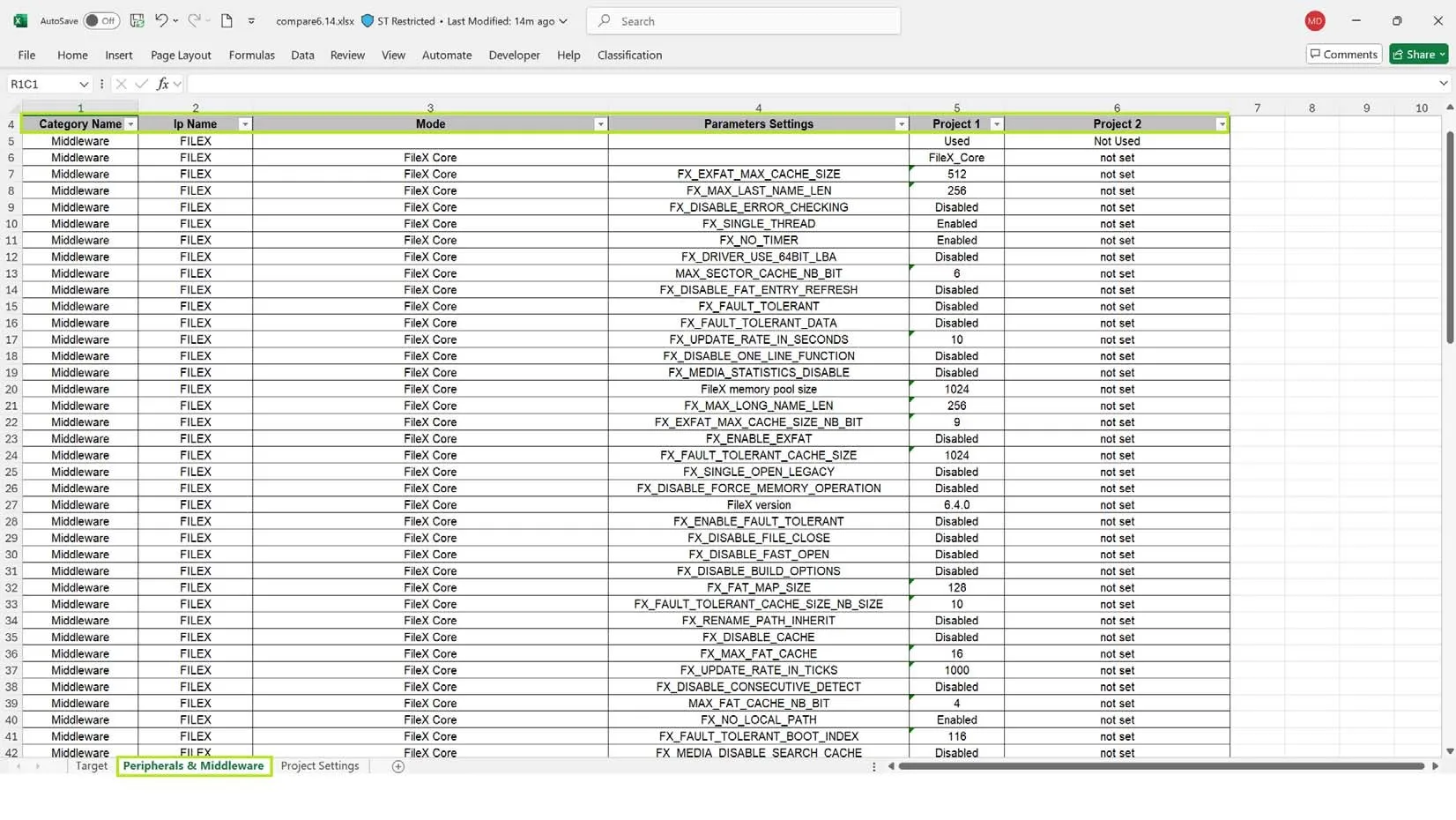
Peripherals & Middleware table ( Figure 368): displays the differences and similarities in the configuration of each peripheral or middleware used in the two projects (the subparameters and the corresponding values).
The data are presented by lines. It is composed of the following columns:
Category name
IP name
Mode
Parameters settings
Project 1
Project 2
The table includes a highlighting feature, which uses color coding to visually differentiate parameters:
Specific parameters for project 1 are marked in blue color
Specific parameters for project 2 are marked in pink color
The common parameters for the two projects are marked in black color
All peripheral categories are displayed collectively, with the option of sorting in alphabetical order.
Project Settings table ( Figure 369), helping the users to know the software environment required for each project, and to determine the necessary tools for ensuring project compatibility and facilitating migration. The table contains information about the firmware package used for each MCU and about the toolchain used for building each project.
It is composed of three columns:
Settings:
CustomerFirmwarePackage
FirmewarePackage
ProjectStructure
TargetToolchain
Project 1
Project 2
5.2.4 Saving the comparison result of the two projects 
In the user interface of the “Compare Projects” tool, there is an Export button that allows users to save the result of the comparison in an external Excel file.
By clicking the Export button, a window named Save appears to allow the user to choose a name for the resulting file and save it ( Figure 370).
The available format:
The result is exported into three sheets in an Excel format (Figure 371).
Each sheet represents a table (Target, Peripherals & Middleware, Projects Settings).
If the user wants to get only the differences in the exported file, they should click on “Show differences only”.
Figure 370. Choosing the Excel format to save the comparison result 
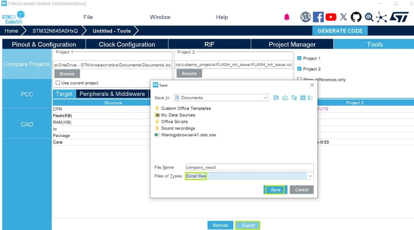
Figure 372. Comparison result in Excel format - Peripherals and middleware 
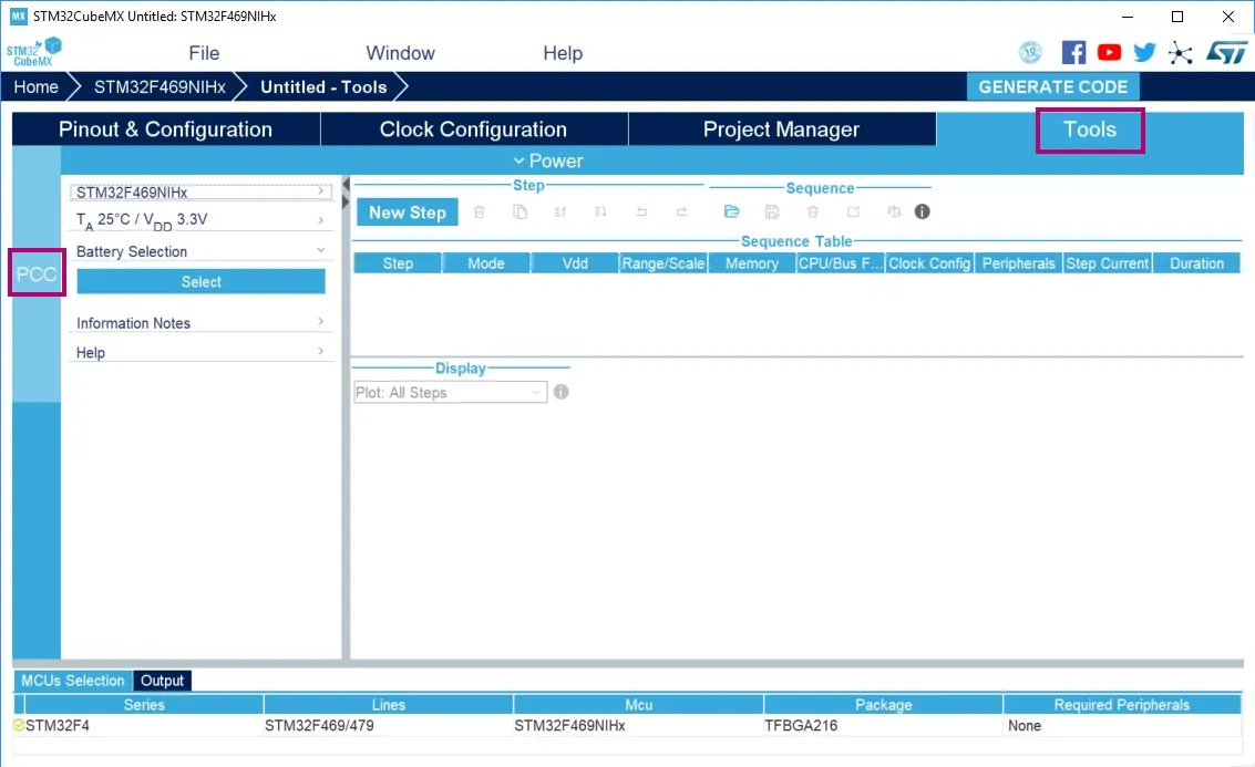
5.3 Power Consumption Calculator view 
For an ever-growing number of embedded systems applications, power consumption is a major concern. To help minimizing it, STM32CubeMX offers the Power Consumption Calculator tab (see Figure 374), which, given a microcontroller, a battery model and a user-defined power sequence, provides the following results:
Average current consumption
Power consumption values can be taken from the datasheet or interpolated from a user specified bus or core frequency.
Battery life
Average DMIPs
DMIPs values are directly taken from the MCU datasheet and are neither interpolated nor extrapolated.
Maximum ambient temperature (TAMAX)
According to the chip internal power consumption, the package type, and a maximum junction temperature of 105 °C, the tool computes the maximum ambient temperature to ensure good operating conditions.
Current T AMAX implementation does not account for I/O consumption. For an accurate estimate, I/O consumption must be specified using the Additional Consumption field. The formula for I/O dynamic current consumption is specified in the microcontroller datasheet.
The Power Consumption Calculator view allows developers to visualize an estimate of the embedded application consumption and lower it further at each power sequence step:
make use of low power modes when available
adjust clock sources and frequencies based on the step requirements • enable only the peripherals necessary for each phase.
For each step the user can choose V BUS as possible power source instead of the battery, impact battery life. If power consumption measurements are available at different voltage levels, STM32CubeMX also proposes a choice of voltage values (see Figure 377).
An additional option, the transition checker, is available for STM32L0, STM32L1, STM32L4, STM32L4+, STM32G0, STM32G4, STM32H7 and STM32WB series. When enabled, the transition checker detects invalid transitions within the currently configured sequence. It ensures that only possible transitions are proposed to the user when a new step is added.
5.3.1 Building a power consumption sequence 
The default starting view is shown in Figure 374.
Figure 374. Power Consumption Calculator default view 
Selecting a VDD value
From this view and when multiple choices are available, the user must select a V DD value.
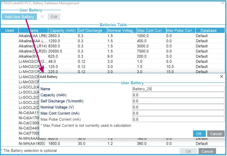
Selecting a battery model (optional) 
Optionally, the user can select a battery model. This can also be done once the power consumption sequence is configured.
The user can select a predefined battery or choose to specify a new battery that best matches its application (see Figure 375).
Figure 375. Battery selection
Power sequence default view
The user can now proceed and build a power sequence.
Managing sequence steps 
Steps can be reorganized within a sequence ( Add new, Delete a step, Duplicate a step, move Up or Down in the sequence) using the set of Step buttons (see Figure 376).
The user can undo or redo the last configuration actions by clicking the Undo button in the Power Consumption Calculator view or the Undo icon from the main toolbar
Figure 376. Step management functions

Adding a step 
There are two ways to add a new step:
Click Add in the Power Consumption panel. The New Step window opens with empty step settings.
Or, select a step from the sequence table and click Duplicate. A New Step window opens duplicating the step settings (see Figure 377).
Figure 377. Power consumption sequence: New Step default view
Editing a step
To edit a step, double-click it in the sequence table, this opens the Edit Step window.
Moving a step 
By default, a new step is added at the end of a sequence. Click the step in the sequence table to select it and use the Up and Down buttons to move it elsewhere in the sequence. Deleting a step
Select the step to be deleted and click the Delete button.
Using the transition checker 
Not all transitions between power modes are possible. The Power Consumption Calculator power menu proposes a transition checker to detect invalid transitions or restrict the sequence configuration to only valid transitions.
Enabling the transition checker option prior to sequence configuration ensures that the user will be able to select only valid transition steps.
Enabling the transition checker option on an already configured sequence will highlight the sequence with a green frame if all transitions are valid (see Figure 378), or in fuchsia if at least one transition is invalid (fuchsia frame with description of invalid step highlighted in fuchsia, see Figure 379). In the latter case, the user can click the Show log button to find out how to solve the transition issue (see Figure 380).
Figure 378. Enabling the transition checker option on an already configured sequence - All transitions valid
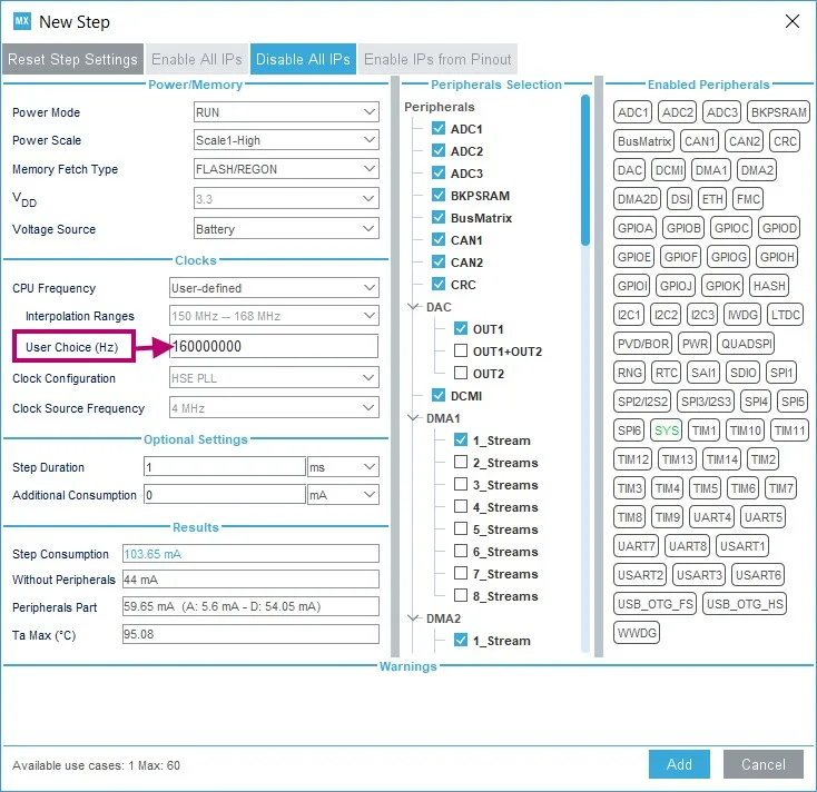
5.3.2 Configuring a step in the power sequence 
The step configuration is performed from the Edit Step and New Step windows. The graphical interface guides the user by forcing a predefined order for setting parameters.
Their naming may differ according to the selected MCU series. For details on each parameter, refer to glossary in Section 5.3.4 and to Appendix C, or to the electrical characteristics section of the datasheet.
The parameters are set automatically by the tool when there is only one possible value (in this case, the parameter cannot be modified and is grayed out). The tool proposes only the configuration choices relevant to the selected MCU.
To configure a new step:
Click Add or Duplicate to open the New step window or double-click a step from the sequence table to open the Edit step window.
Within the open step window, select in the following order:
The Power Mode
Changing the Power Mode resets the whole step configuration.
The Peripherals
Peripherals can be selected/deselected at any time after the Power Mode is configured.
The Power scale
The power scale corresponds to the power consumption range (STM32L1) or the power scale (STM32F4).
Changing the Power Mode or the Power Consumption Range discards all subsequent configurations.
The Memory Fetch Type
The VDD value if multiple choices available
The voltage source (battery or VBUS)
A Clock Configuration
Changing the Clock Configuration resets the frequency choices further down.
When multiple choices are available, the CPU Frequency (STM32F4) and the AHB Bus Frequency/CPU Frequency(STM32L1) or, for active modes, a user specified frequency. In this case, the consumption value will be interpolated (see Using interpolation).
Optionally set
A step duration (1 ms is the default value)
An additional consumption value (expressed in mA) to reflect, for example, external components used by the application (external regulator, external pull-up, LEDs or other displays). This value added to the microcontroller power consumption will impact the step overall power consumption.
Once the configuration is complete, the Add button becomes active. Click it to create the step and add it to the sequence table.
Using interpolation 
For steps configured for active modes (Run, Sleep), frequency interpolation is supported by selecting CPU frequency as User Defined and entering a frequency in Hz (see Figure 381).
Figure 381. Interpolated power consumption
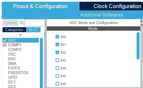
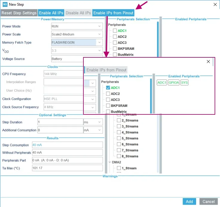
Importing pinout 
Figure 382 illustrates the example of the ADC configuration in the Pinout view: clicking Enable IPs from Pinout in the Power Consumption Calculator view selects the ADC peripheral and GPIO A ( Figure 383).
The Enable IPs from Pinout button allows the user to automatically select the peripherals that have been configured in the Pinout view.
Selecting/deselecting all peripherals 
Clicking Enable All IPs allows the user to select all peripherals at once.
Clicking Disable All IPs removes them as contributors to the consumption.
Figure 383. Power Consumption Calculator configuration window:
ADC enabled using import pinout
5.3.3 Managing user-defined power sequence and reviewing results 
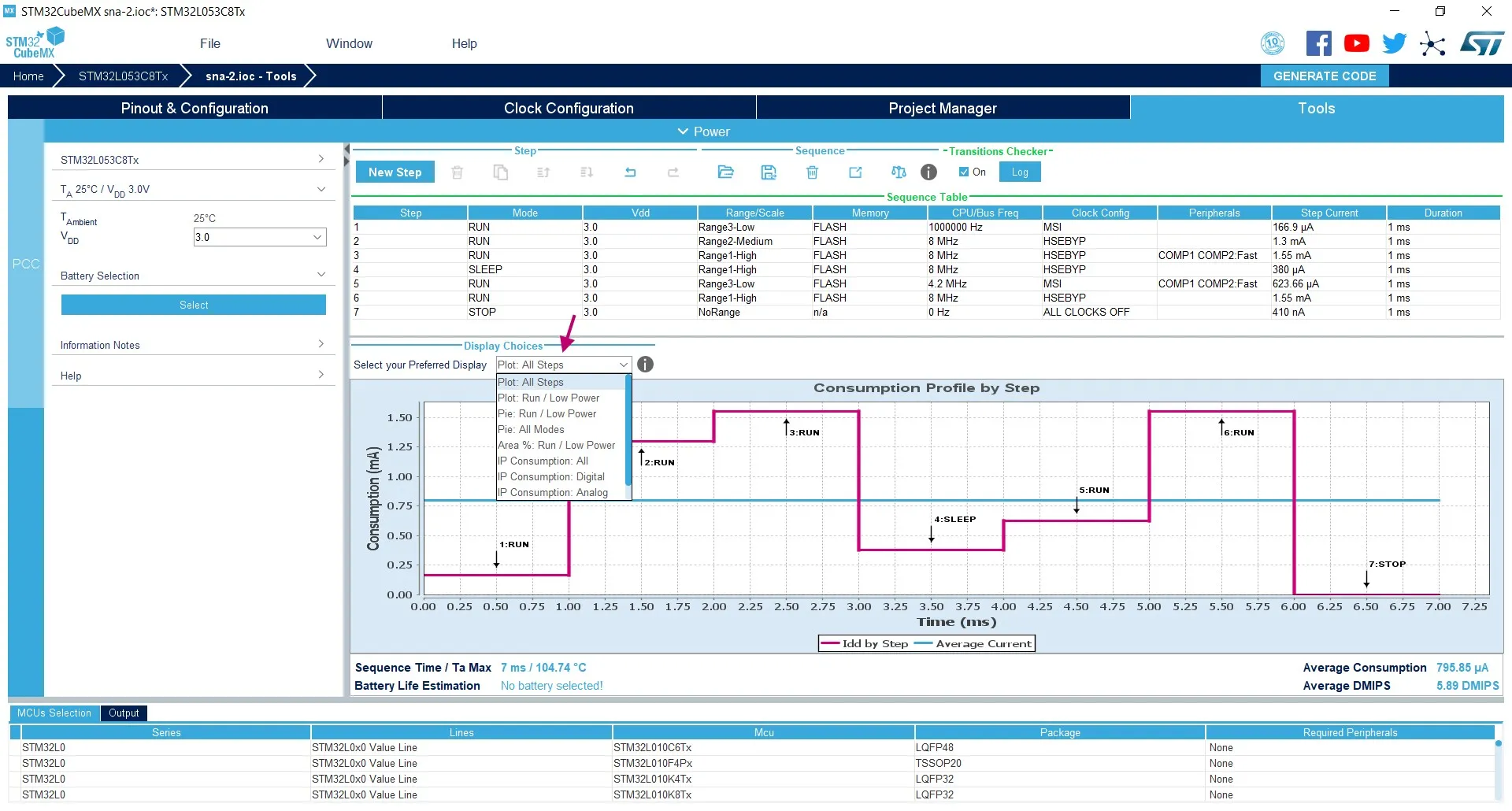
The configuration of a power sequence leads to an update of the Power Consumption Calculator view (see Figure 384):
The sequence table shows all steps and step parameters values. A category column indicates whether the consumption values are taken from the datasheet or are interpolated.
The sequence chart area shows different views of the power sequence according to a display type (e.g. plot all steps, plot low power versus run modes)
The results summary provides the total sequence time, the maximum ambient temperature (TAMAX), plus an estimate of the average power consumption, DMIPS, and battery lifetime provided a valid battery configuration has been selected.
Figure 384. Power Consumption Calculator view after sequence building 
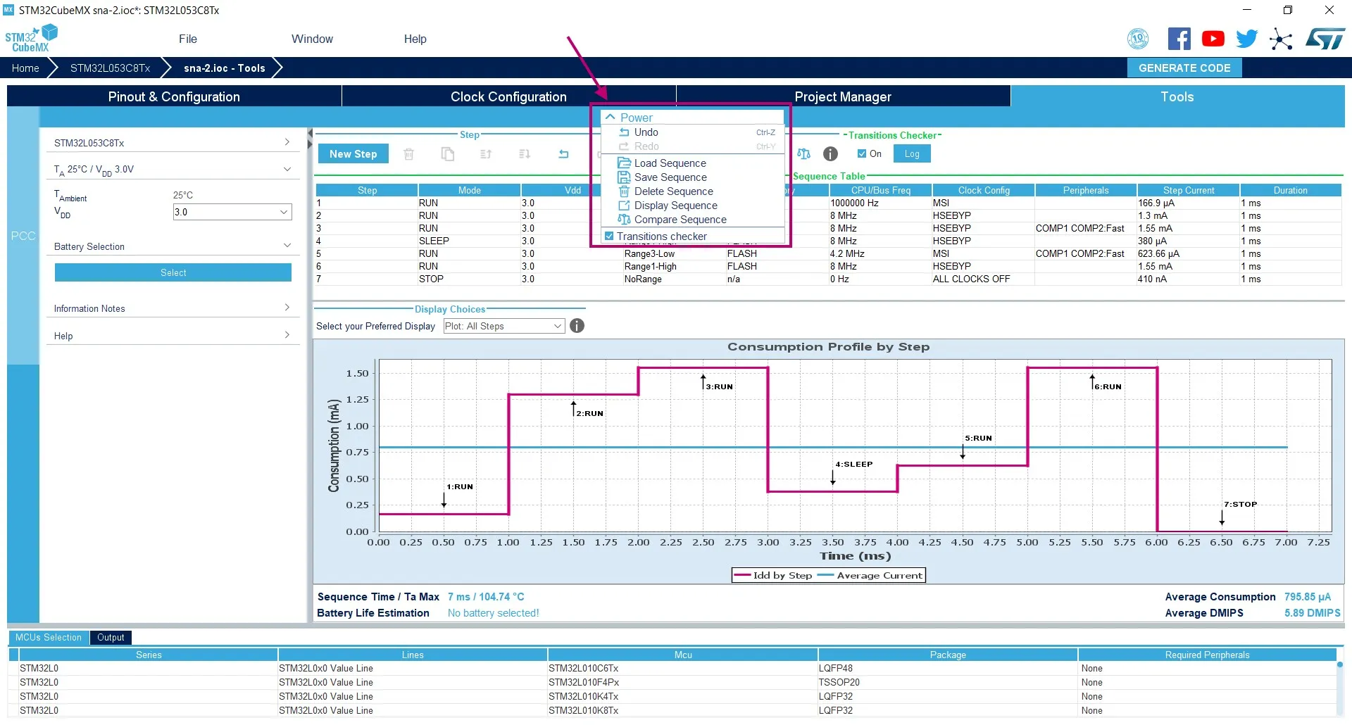
Managing the whole sequence (load, save and compare) 
From the power menu (see Figure 385), the current sequence can be saved, deleted or compared to a previously saved sequence that will be displayed in a dedicated popup window.
Figure 385. Sequence table management functions
Managing the results charts and display options 
In the Display area, select the type of chart to display (e.g. sequence steps, pie charts, consumption per peripherals). You can also click External Display to open the charts in dedicated windows (see Figure 386).
Right-click on the chart to access the contextual menus: Properties, Copy, Save as png picture file, Print, Zoom menus, and Auto Range to reset to the original view before zoom operations. Zooming can also be achieved by mouse selecting from left to right a zone in the chart and Zoom reset by clicking the chart and dragging the mouse to the left.
Figure 386. Power Consumption: Peripherals consumption chart
Overview of the Results summary area 
This area provides the following information (see Figure 387):
Total sequence time, as the sum of the sequence steps durations.
Average consumption, as the sum of each step consumption weighed by the step duration.
The average DMIPS (Dhrystone million instructions per second) based on Dhrystone benchmark, highlighting the CPU performance for the defined sequence.
Battery life estimation for the selected battery model, based on the average power consumption and the battery self-discharge.
TAMAX: highest maximum ambient temperature value found during the sequence.
Figure 387. Description of the Results area

5.3.4 Power sequence step parameters glossary 
The parameters that characterize power sequence steps are the following (refer to Appendix C: STM32 microcontrollers power consumption parameters for more details):
Power modes
To save energy, it is recommended to switch the microcontroller operating mode from running mode, where a maximum power is required, to a low-power mode requiring limited resources.
VCORE range (STM32L1) or Power scale (STM32F4)
These parameters are set by software to control the power supply range for digital peripherals.
Memory Fetch Type
This field proposes the possible memory locations for application C code execution. It can be either RAM, FLASH or FLASH with ART ON or OFF (only for families that feature a proprietary Adaptive real-time (ART) memory accelerator which increases the program execution speed when executing from flash memory).
The performance achieved thanks to the ART accelerator is equivalent to 0 wait state program execution from flash memory. In terms of power consumption, it is equivalent to program execution from RAM. In addition, STM32CubeMX uses the same selection choice to cover both settings, RAM and flash memory with ART ON.
Clock Configuration
This operation sets the AHB bus frequency or the CPU frequency that will be used for computing the microcontroller power consumption. When there is only one possible choice, the frequencies are automatically configured.
The clock configuration drop-down list allows to configure the application clocks:
the internal or external oscillator sources: MSI, HSI, LSI, HSE or LSE
the oscillator frequency
other determining parameters, among them PLL ON, LSE Bypass, AHB prescaler value, LCD with duty
Peripherals
The peripheral list shows the peripherals available for the selected power mode. The power consumption is given assuming that peripherals are only clocked (e.g. not in use by a running program). Each peripheral can be enabled or disabled, their individual power consumption is displayed in a tooltip. An overall consumption due to peripheral analog and digital parts is provided in the step Results area (see Figure 388).
Figure 388. Overall peripheral consumption
none (Disable All)
some (using peripheral dedicated checkbox)
all (Activate All)
or all from the previously defined pinout configuration (Import Pinout).
Only the selected and enabled peripherals are taken into account when computing the power consumption.
Step duration
The user can change the default step duration value. When building a sequence, the user can either create steps according to the application actual power sequence or define them as a percentage spent in each mode. For example, if an application spends 30% in Run mode, 20% in Sleep and 50% in Stop, the user must configure a 3-step sequence consisting in 30 ms in Run, 20 ms in Sleep and 50 ms in Stop.
Additional consumption
This field allows entering an additional consumption resulting from specific user configuration (e.g. MCU providing power supply to other connected devices).
5.3.5 Battery glossary 
Capacity (mAh)
Amount of energy that can be delivered in a single battery discharge.
Self-discharge (% / month)
This percentage, over a specified period, represents the loss of battery capacity when the battery is not used (open-circuit conditions), as a result of internal leakage.
Nominal voltage (V)
Voltage supplied by a fully charged battery.
Max. continuous current (mA)
This current corresponds to the maximum current that can be delivered during the battery lifetime period without damaging the battery.
Max. pulse current (mA)
This is the maximum pulse current that can be delivered exceptionally, for instance when the application is switched on during the starting phase.
5.3.6 SMPS feature 
Some microcontrollers (e.g. STM32L496xxxxP) allow the user to connect an external switched mode power supply (SMPS) to further reduce power consumption.
For such microcontrollers, the Power Consumption Calculator tool offers the following features:
Selection of SMPS for the current project
From the left panel, check the Use SMPS box to use SMPS (see Figure 389). By default, ST SMPS model is used.
Selection of another SMPS model by clicking the Change button
This opens the SMPS database management window in which the user can add a new SMPS model (see Figure 390). The user can then select a different SMPS model for the current sequence (see Figure 391, Figure 392 and Figure 393)
Check for invalid SMPS transitions in the current sequence by enabling the SMPS checker
To do this, select the checkbox to enable the checker and click the Help button to open the reference state diagram (see Figure 394).
Configuration of SMPS mode for each step (see Figure 395)
If the SMPS checker is enabled, only the SMPS modes valid for the current step are proposed.
Figure 389. Selecting SMPS for the current project 
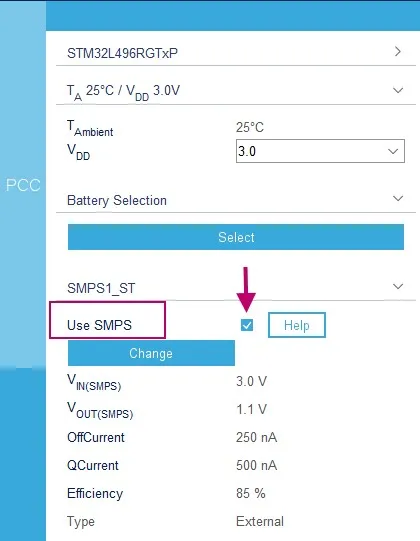
Figure 390. SMPS database - Adding new SMPS models 
Figure 392. Current project configuration updated with new SMPS model 
Figure 394. SMPS transition checker and state diagram helper window 
Figure 395. Configuring the SMPS mode for each step 
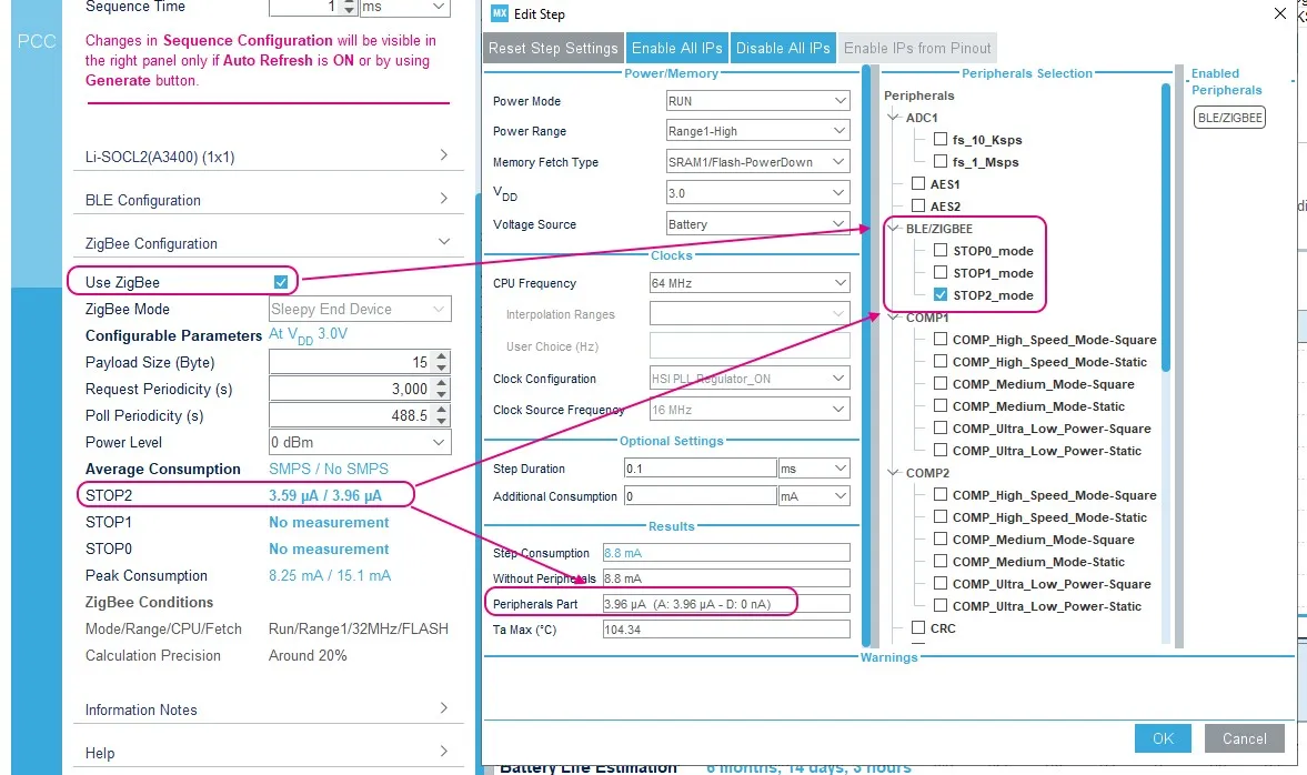
5.3.7 Bluetooth Low-Energy ® /ZigBee ® support (STM32WB series only) 
The Power Consumption tool allows the user to take into account the consumption related to the RF peripheral and corresponding Bluetooth Low-Energy functional mode, combined with the usage of the SMPS feature.
Figure 397. RF Bluetooth Low-Energy mode configuration (STM32WB series only) 
5.3.8 Sub-GHz support (STM32WL series only) 
Sub-GHz usage can be enabled from the left panel and configured to reflect the application relevant settings. For each new step enabling ZigBee, the peripheral consumption part is updated accordingly (see Figure 399).
5.3.9 Example feature (STM32MPUs and STM32H7 dual-core only) 
Under the section Sequence Examples, the PCC tool allows to access examples: each of them comes with an explanatory slide set and a ready-made sequence to load in PCC (see Figure 400).
Figure 400. Power Consumption Calculator - Example set 
Figure 402. Power Consumption Calculator - Example sequence new selection 
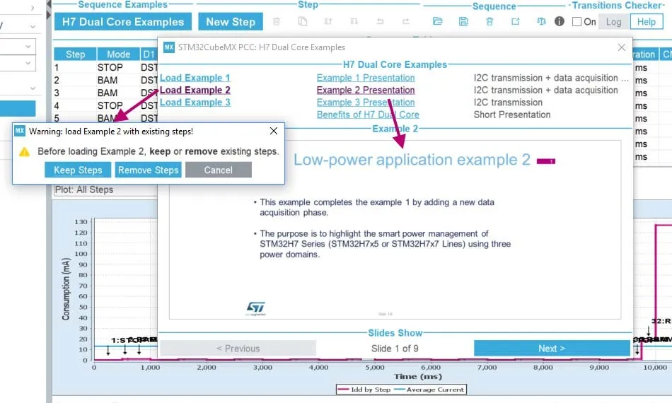
Note: The examples are provided for a given part number and may require adjustments when used for a different part number. Also, after loading, it is recommended to edit each step and check settings.
5.4 DDR Suite (STM32MPUs only) 
DDR SDRAMs are complex high speed devices that need careful PCB design.
The STM32MP15 devices support the following DDR types:
LPDDR2
LPDDR3
DDR3 / DDR3L
They are specified by the JEDEC standard (standardization of interfaces, commands, timings, packages and ballout).
STM32CubeMX has been extended to provide an exhaustive tool suite for the DDR subsystem. It proposes the following key features.
Configuration of DDR controller and PHY registers is managed automatically based on reduced set of editable parameters.
DDR testing is offered based on a rich list. Tests go from basic to stress. User can also develop its own tests.
DDR configuration is accessible like the other peripherals in the Pinout & Configuration view: clicking the DDR from the component panel opens the mode and configuration panels.
DDR Test suite testing and tuning features are available from the Tools view.
The DDR suite relies on two important concepts:
the DDR timings as key inputs for the configuration of the DDR Controller and PHY
the tuning of DDR signals to compensate board design imperfections.
5.4.1 DDR configuration 
STM32CubeMX allows to set DDR system parameters and JEDEC core timings. The timing parameters are available in the DDR datasheet.
DDR type, width, and density 
The DDR type, width, and density parameters must be set to proceed with the DDR configuration. This can be done in the Mode panel after selecting the DDR in the Pinout & Configuration view. See Figure 403 for an example of LPDDR2 settings.
Figure 403. DDR pinout and configuration settings
Note: Contexts for DDR IP cannot be changed, DDR is tied to “Cortex-A7 nonsecure” identified as “Cortex-A7 NS” in the tool. DDR configuration
Clicking on a parameter will show additional details in the DDR configuration footer. - The DDR frequency is taken from the ‘Clock configuration’ tab, it cannot be changed in the DDR configuration.
The ‘Relaxed Timing’ mode is used during bring-up phase for trying relaxed key DDR timings value (one tCK added to tRC, tRCD and tRP timings)
Other parameters must be retrieved from the user DDR datasheet. • Some parameters are read-only: they are for information only and depend on the DDR type.
Clicking “generate code” automatically computes the DDR node of the device tree (DDR Controller and DDR PHY registers values) based on these parameters.
DDR3 configuration 
For DDR3, the configuration is made easier with the selection of a Speed Bin Grade combination, instead of manually editing timing parameters.
Figure 404. DDR3 configuration
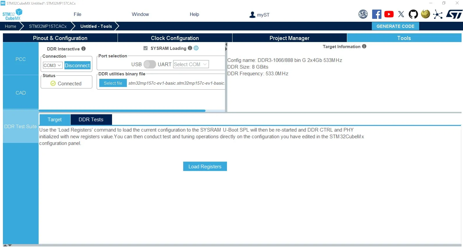
5.4.2 Connection to the target and DDR register loading 
To manage DDR tests and tuning, STM32CubeMX must establish a connection with the target and more specifically with U-Boot SPL using the DDR interactive protocol:
the DDR interactive protocol is only available in the Basic boot scheme U-Boot SPL binary and supported over the UART4 peripheral instance
when U-Boot SPL detects a connection to STM32CubeMX on UART4, it stops its initialization process and accepts commands from STM32CubeMX.
There are two connection options:
the U-Boot SPL binary is available in flash memory
the U-Boot SPL needs to be loaded in SYSRAM because the DDR has not yet been tested nor tuned (and, consequently, is not fully functional yet).
Prerequisites 
Installation of ST-Link USB driver to perform firmware upgrades: for Windows, latest version of STSW-LINK009, for Linux, use STSW-LINK007. Both can be downloaded from www.st.com.
Installation of STM32CubeProgrammer (for SYSRAM loading only): installer can be downloaded from www.st.com.
Connection to the target 
The COM port must be selected to connect to the target, as indicated in Figure 405.
Figure 405. DDR Suite - Connection to target
Output/Log messages 
STM32CubeMX outputs DDR suite related activity logs (see Figure 407) and interactive protocol communication logs (see Figure 408). They are displayed by enabling outputs from the Window menu.
DDR register loading (optional) 
Once connected in DDR interactive mode, the current DDR configuration can be loaded in
SYSRAM.
5.4.3 DDR testing 
Prerequisites 
To proceed with DDR testing:
The DDR suite must be in connected state
The DDR configuration must be available in memory, either with the U-Boot SPL (with DDR register file in Device Tree) or in the DDR registers (see Section 5.4.2).
DDR test list 
DDR tests are part of the U-Boot SPL (see Figure 410).
Figure 410. DDR test list from U-Boot SPL
On STM32MP15, DDR base address is 0xC0000000 (as an example, DDR size for 4 Gbits is 0x20000000). • Loop: number of test iterations before verdict. Same test is repeated [Loop] times. Verdict OK if all tests are OK, KO otherwise.
Size: the byte size of the region to test. It must be a multiple of 4 (read/writes are performed on 32-bit unsigned integers), with minimal value equal to 4, and up to DDR size.
Pattern: the 32-bit pattern to be used for read / write operations.
The DDR Suite embeds an auto-correction feature preventing users to specify wrong values.
All tests are performed with Data cache disabled and Instruction cache enabled.
DDR test results 
The test verdict is reported by the U-Boot SPL: the parameters used for the tests are recalled, along with Pass/Fail status and results details (see Figure 411). The test history is available in the output and Logs panels (see Figure 412).
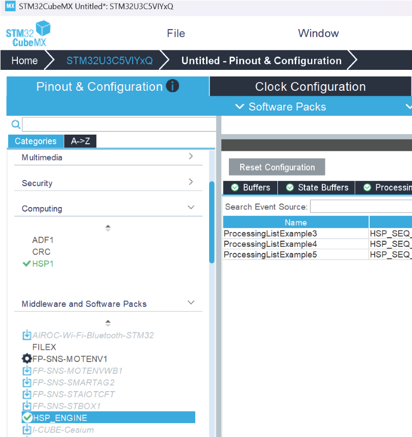
5.5 STM32CubeMX Memory Management Tool 
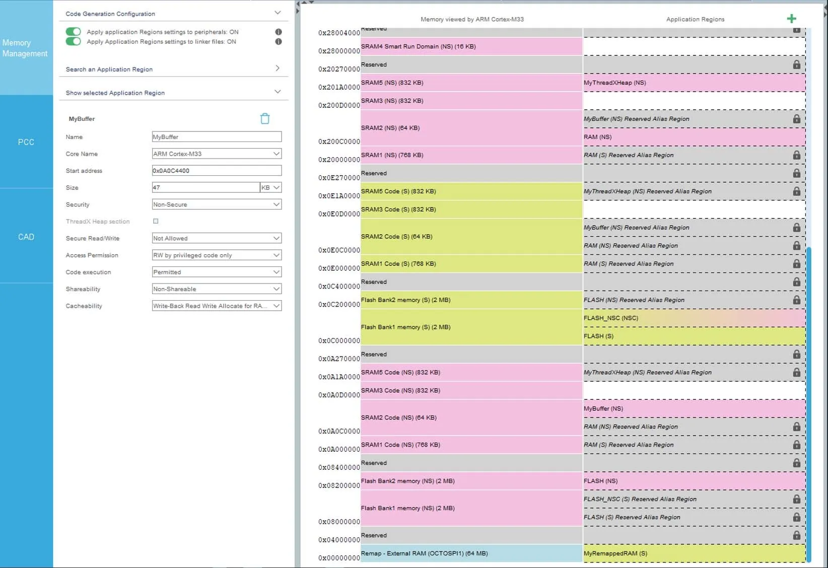
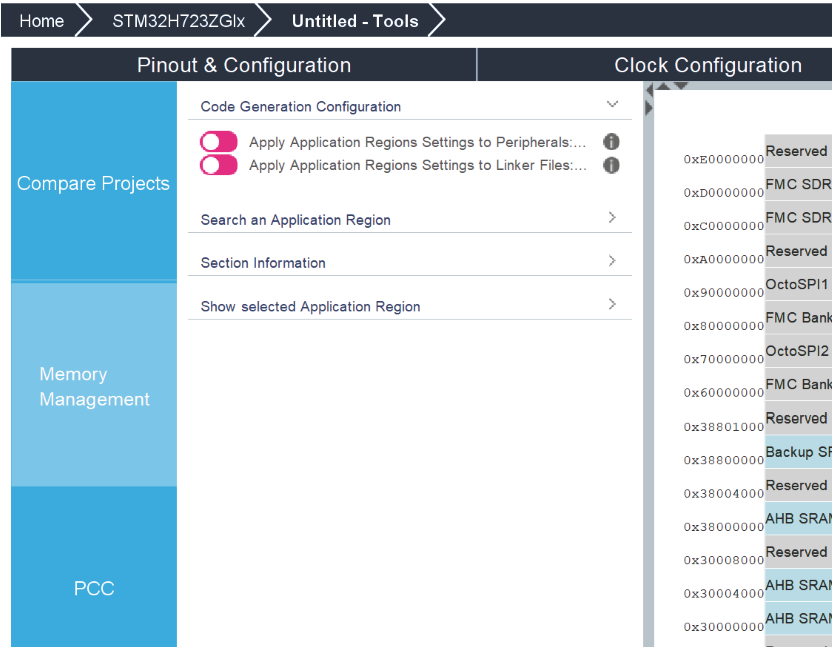
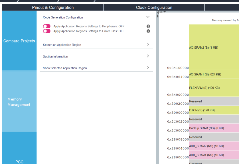
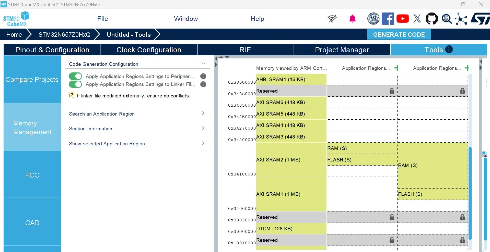
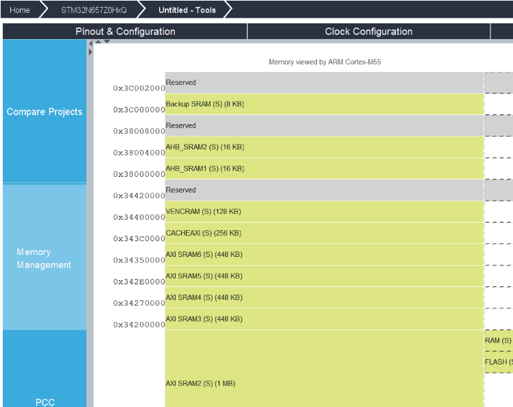
The Memory Management Tool (MMT) displays the memory map and defines memory attributes applied in user projects opened/created in STM32CubeMX.
The tool is located in the “Tools” tab. It allows the user to declare memory regions (referred to as application regions or AppReg) at application level.
The HW constraints related to TrustZone, Memory Protection Unit, and the memory granularity are handled by MMT and made transparent to the user, so that the focus can be put on the memory regions. A linker file is generated according to the application regions declared and configured by the user.
The MMT key features are:
Memory map display
Application regions management
Linker file generation
MMT interacts with peripherals starting from the moment the user enters its interface:
Checks their settings
Updates other peripherals involved in memory map configuration The peripherals are updated only when the first toggle button is ON.
Figure 413. Regions settings to peripherals ON
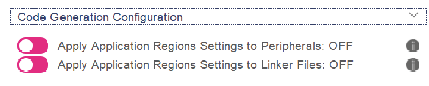
Figure 416. Recommendation for the configuration of MMT 
5.5.1 STM32H5, STM32U3, STM32U5, STM32WBA5, STM32WBA5M,
and STM32WBA6 with TrustZone activated 
Feature: MMT usage, pinout, and configuration user interface 
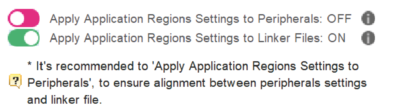
When the first toggle button is ON (see Figure 413), SAU, GTZC, Cortex-M33 (MPU), and FLASH configurations are under MMT control: their modes and parameters become read-only.
Feature: MMT usage and linker script 

MS81244V1
Linker files contents are generated as the MMT is used.
For the following features: SAU, GTZC, Cortex-M33 MPU, and FLASH, the memory handle is not under MMT control, so the user can update their setting.
Figure 418. MMT view
Figure 419. Start a project
Region information 
Clicking on a particular region in the Application Regions column shows the associated details on the left hand side.
You can choose to hide the name of the reserved region, or hide the Secure/Non Secure indication close to the region name (the secure/nonsecure indication is indicated by the color).
Figure 422. Region information
Code generation configuration 
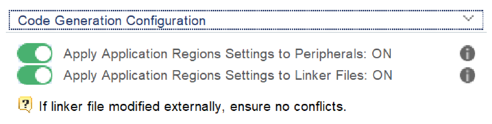
The application regions settings can be applied to peripherals on the left of the screen. The concerned peripherals are shown on the associated tooltip. This can impact their availability on the pinout screen configuration.
Figure 423. Tooltip
Apply Application Regions settings to linker files 
When this button is on, the linker scripts for the secure and non secure applications are generated, taking into account the configuration.
Figure 426. Linker files update
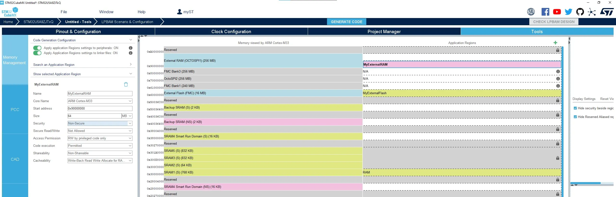
For our example, we need half of the available 128 Mbytes.
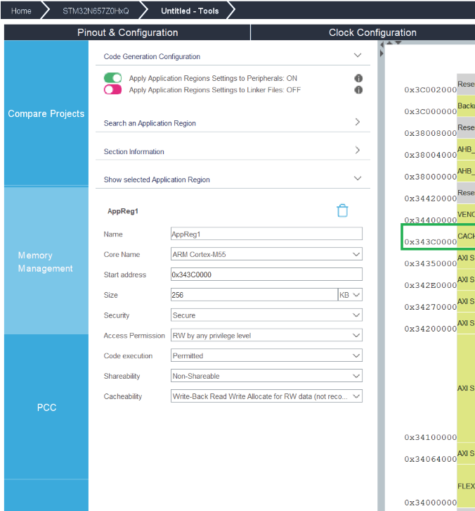
Press the “+” button, set a name for the region (for instance: MyExternalRAM), and put 64 MB for its size.
Figure 431. Memory assignment
Configuring a memory region using the left panel 
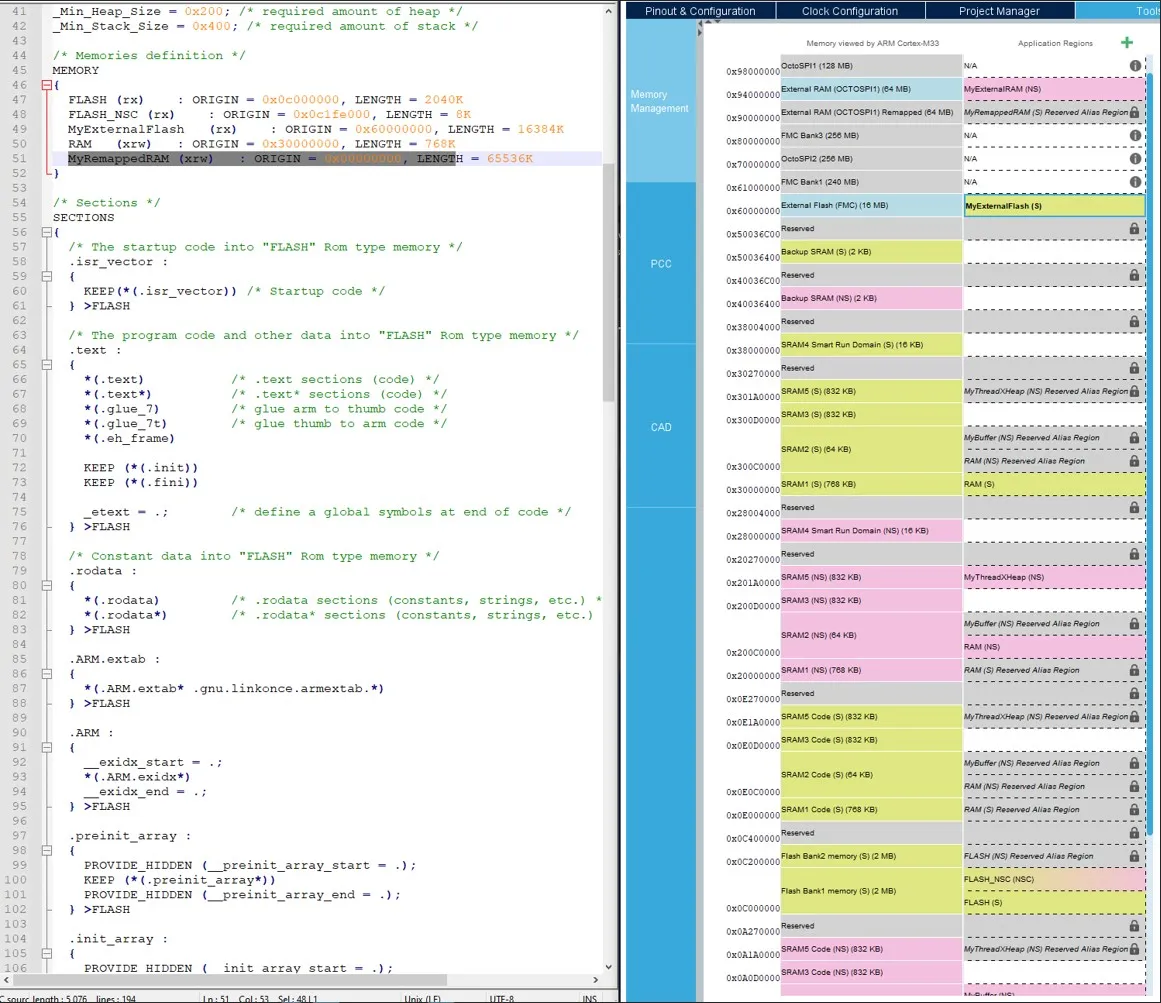
With the left panel (see Figure 432) you can adjust items such as starting position and size. In this example, the added region must be adjusted: we want it to be allocated to the non secure project, and to start in the middle of the RAM. By adjusting those values, the expected results appear (see Figure 433). The color is now pink (nonsecure), and the region starts in the middle of the RAM (OctoSPI1).
Figure 432. Left panel configuration
Setting up a middleware memory location 
The application needs ThreadX. Go back to the “Pinout & Configuration” tab. Choose ThreadX, then use the Use Dynamic Allocation under Memory Configuration.
Figure 434. Middleware memory allocation
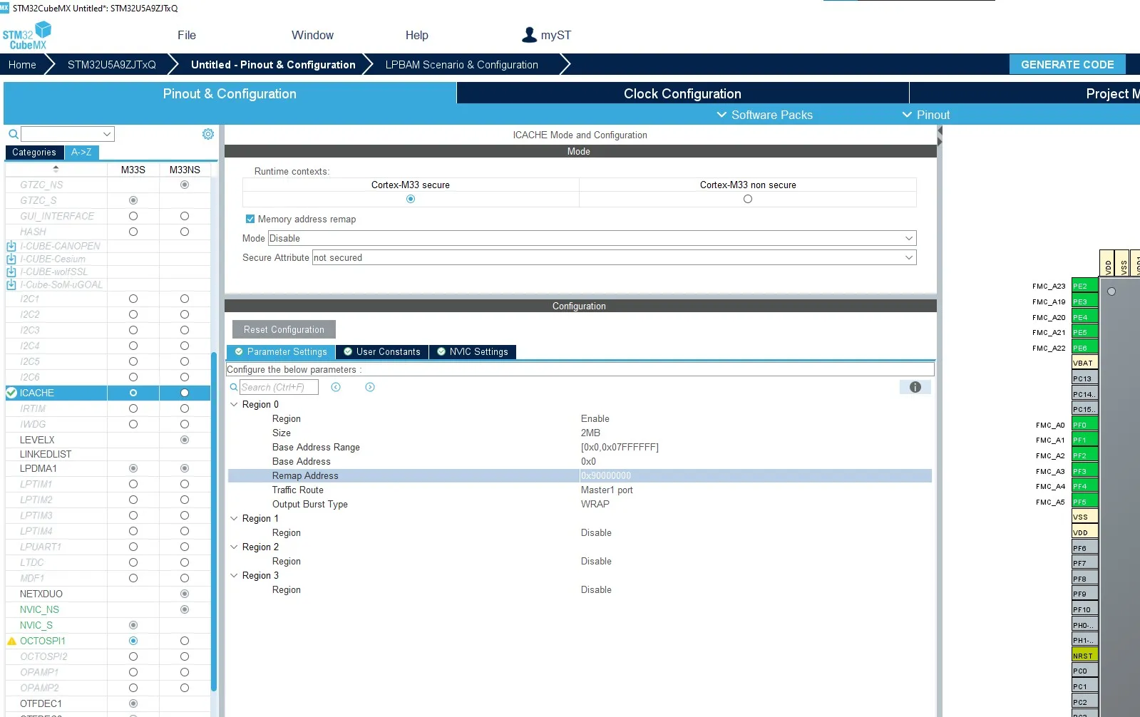
Go to the Pinout & Configuration tab
Enable ICACHE, select the Memory address remap tick box
Select a region and set the memory size to 64 Mbytes
Change the Remap address to 0x9000 0000
Figure 436. Remapping the memory
Go back to the MMT tab. Region 0x9000 0000 is named with Remapped, with the amount of RAM previously selected.
Figure 437. Remapped region is renamed
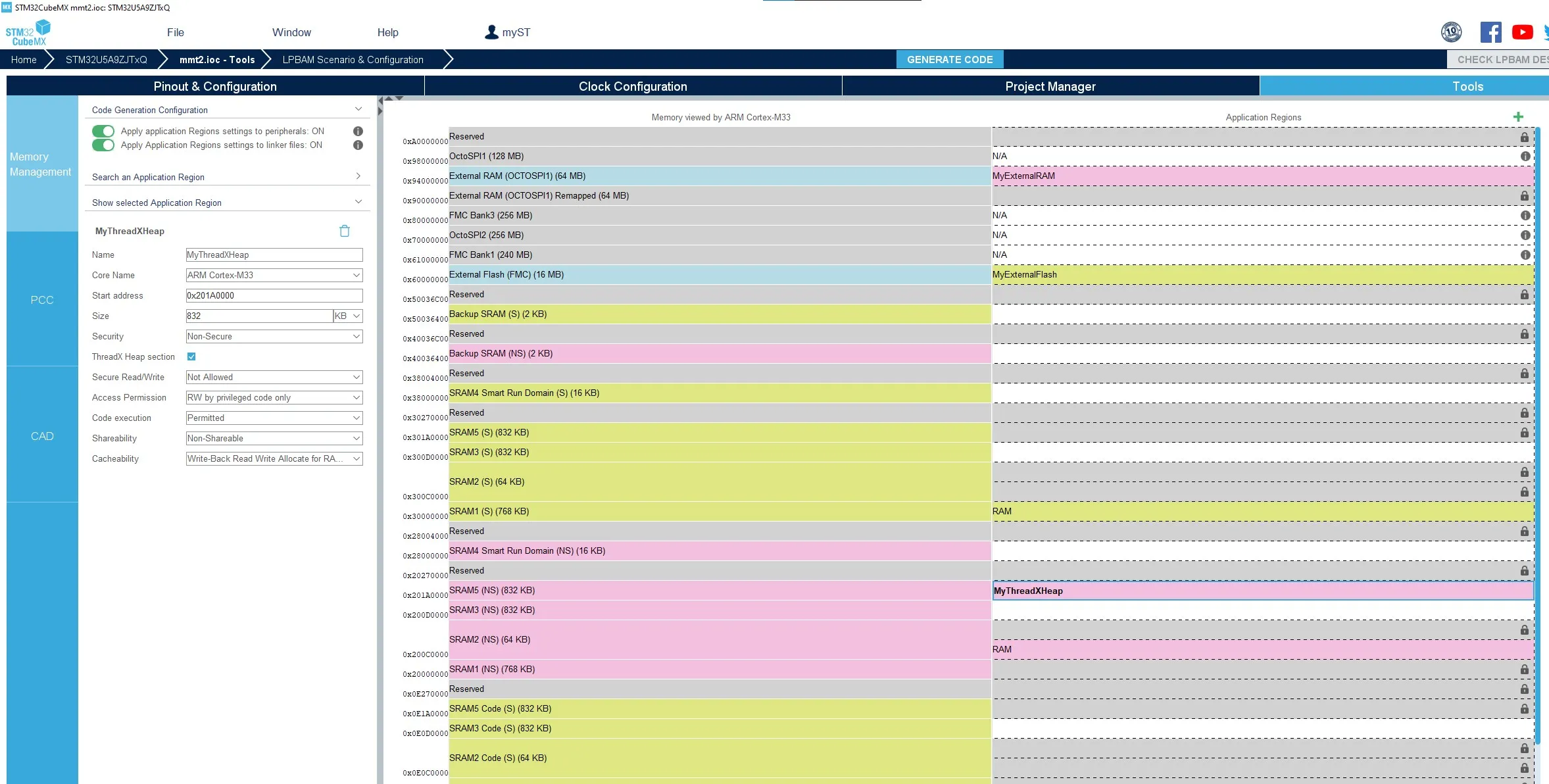
There is also a Remap – External RAM(OCTOSPI1) added at address 0x0000 0000.
Figure 438. Remapped start address
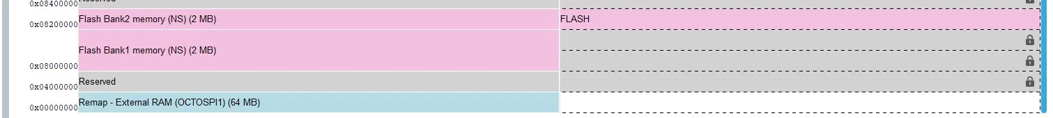
Add a new region named “MyRemappedRAM” at that address.
Figure 439. New region remapped
Code generation 
Go to the project manager, set a name to your project, Choose CubeIDE as a toolchain and press GENERATE CODE
Navigate to the generated Secure Project and open the linker definition file. Under the Memories definition you will see the defined memories with their start address and
length. This file shows only the secure regions in green. Open the nonsecure linker file and check the same location for the memory regions allocated to the nonsecure area.
Figure 442. Memory map in linker file
5.5.3 STM32H7 single core and STM32U5 without TrustZone activated 
Feature: MMT usage, pinout, and configuration user interface 
When the first toggle button is ON, Cortex-M33 (MPU for STM32U5) and Cortex-M7 (MPU for STM32H7) are under MMT control (see, respectively, Figure 443 and Figure 444): modes and parameters become read-only.
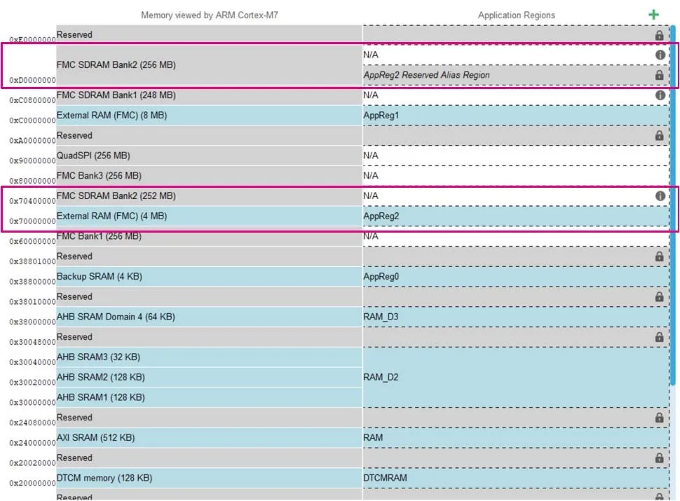
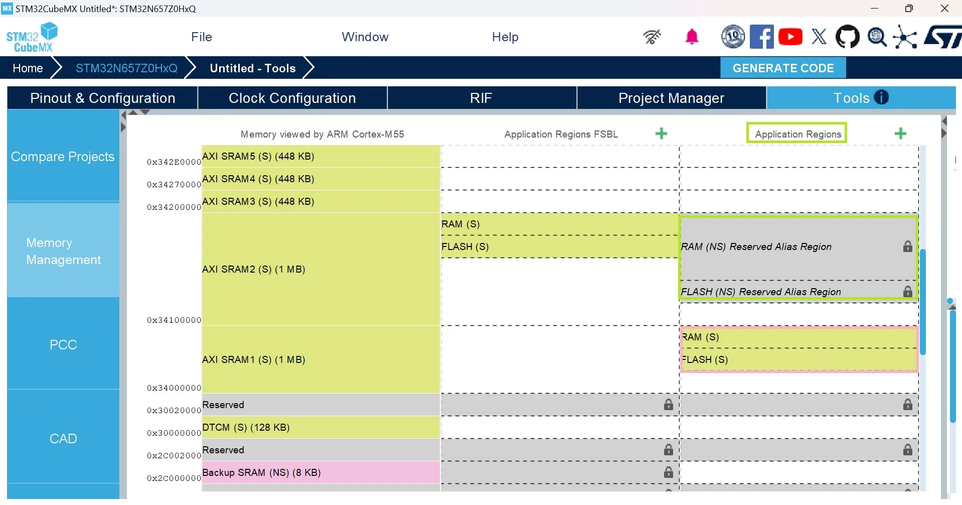
The middle panel (see, respectively, Figure 445 and Figure 446 for STM32U5 and STM32H7) represents the memory, split into two columns: the left one is the memory seen by the core(s), the right one the memory set-up for the application.
For the new project created under STM32CubeMX the tool creates the default application region to generate a valid project.
Figure 443. MMT usage (STM32U5)
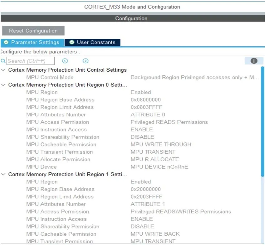
Figure 444. MMT usage (STM32H7 single core)
FMC impact on MMT 
When activating FMC and SDRAM Bank1, a tab mapping (see Figure 448) is displayed, with three options:
Default mapping (see Figure 449): MMT initializes as default position of SDRAM Bank1, SDRAM Bank2, and NOR PSRAM (default viewer of MMT)
NOR/PSRAM bank and SDRAM Bank1/2 are swapped: MMT swaps the position of SDRAM Bank1 and NOR PSRAM Bank1 (see Figure 450 and Figure 451)
SDRAM Bank2 remapped on FMC Bank2 and still accessible at default mapping: MMT updates the position of SDRAM Bank1 to be remapped on position of FMC Bank2 (see Figure 452 and Figure 453)
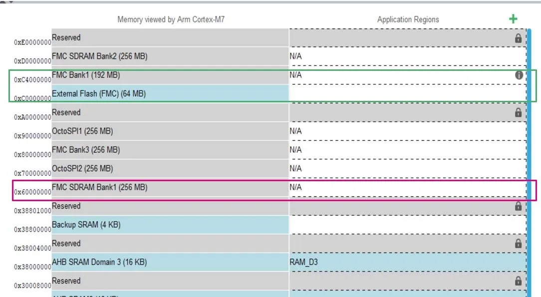
Figure 453. After remapping
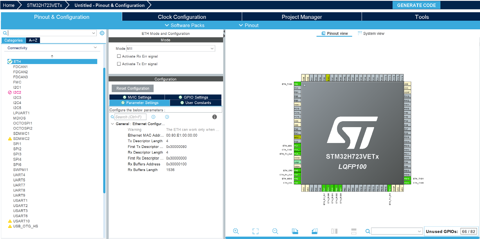
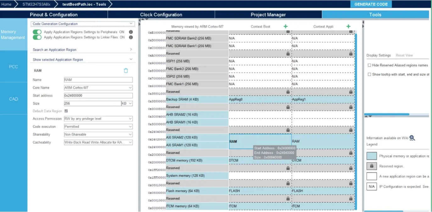
ETH impact on MMT for STM32H7 single core 
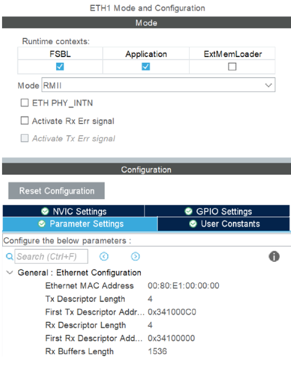
An example of MMT configuration of the ETH IP on the STM32H723VETx MCU
Activate the IP ETH:
MMT creates three application regions within the MMT view.
To change the start address and the size of each region, update the ETH parameters.
Press the radio button “Apply Application region Settings to Peripherals ON”, ETH will be partially under MMT control.
Press the Generate Code button to generate code for both applications.
Apply Application Regions settings to linker files:
When this button is on, the linker scripts are generated, considering the configuration.
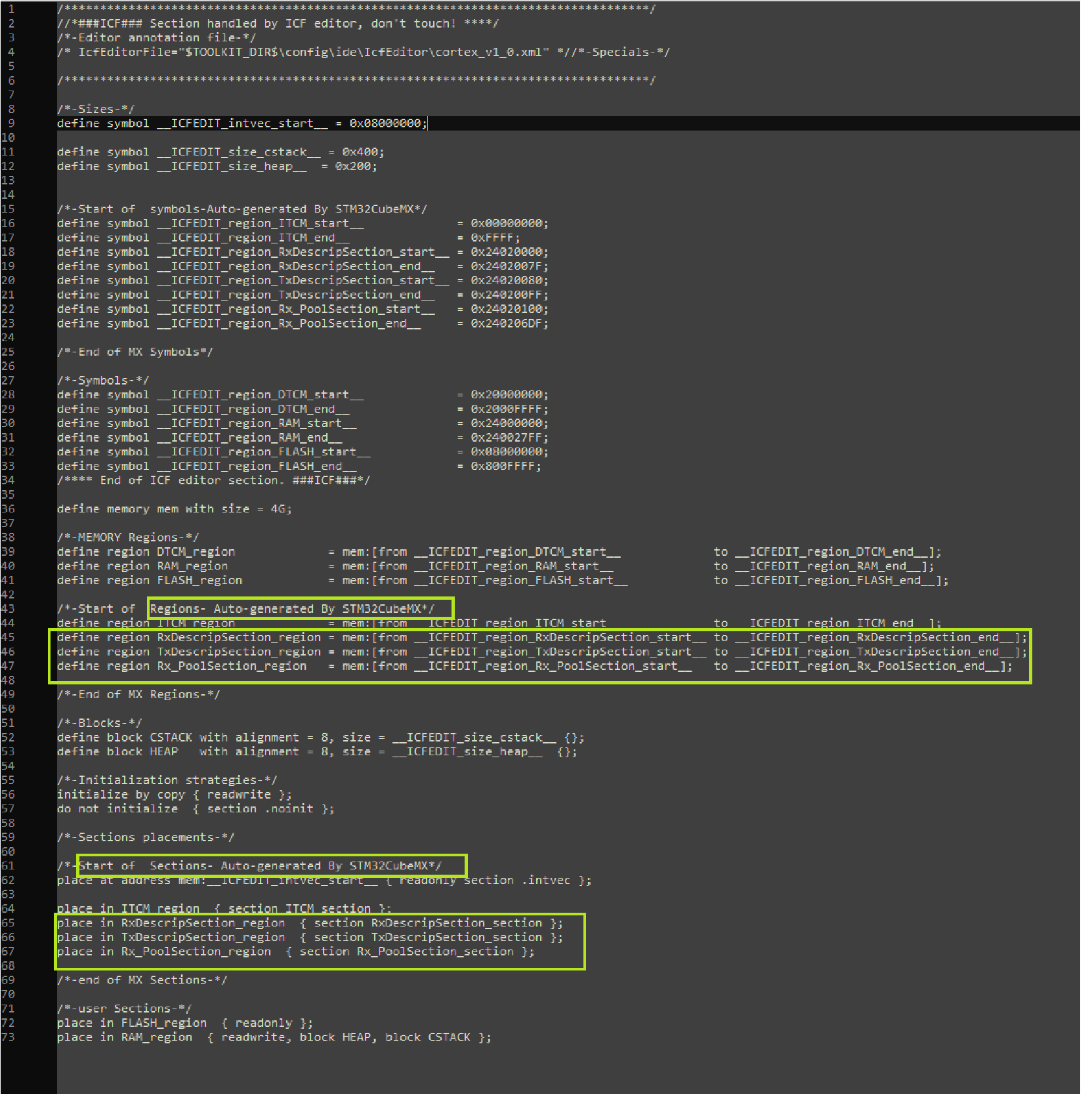
After the code generation, navigate to the generated folder:
Open the linker definition file.
Under the Memories definition you can see the memories with their start address and length, according to the configuration made in STM32CubeMX.
Figure 454. ETH MMT regions
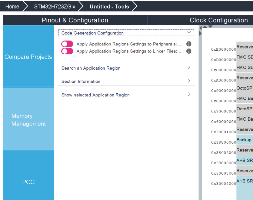
Figure 455. ETH configuration for STM32H723VETx MCU
5.5.4 STM32WBxx 
Feature: MMT usage, pinout, and configuration user interface 
When the first toggle button is ON, Cortex-M33 is under MMT control: its modes and parameters become read-only (see Figure 457).
This example is based on an STM32WB5x MCU, so the list must contain only stm32wb5x_x binaries. The button “Refresh” is used to refresh the binaries list version in the repository of STM32Cube firmware (see Figure 459).
Figure 459. MMT configuration for STM32WB5x
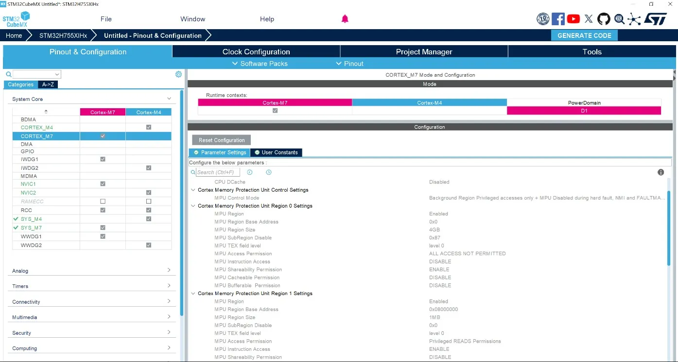
5.5.5 STM32H7 Dual-core without Trust Zone activated 
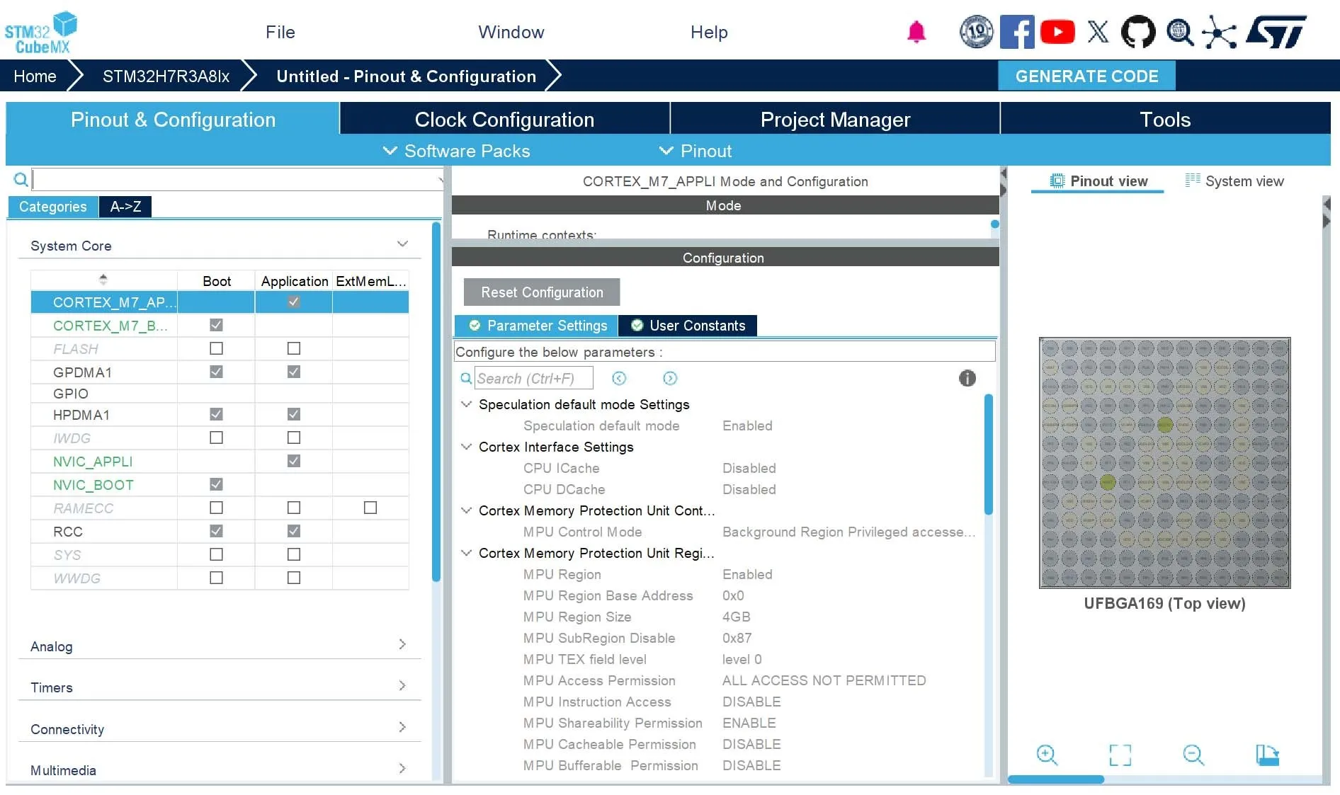
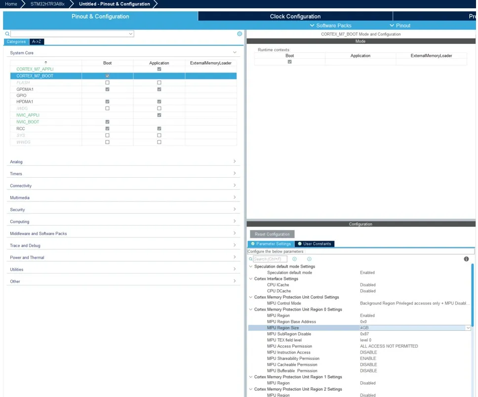
Feature: MMT usage, pinout, and user interface configuration 
When the first toggle button is ON, Cortex-M7_BOOT (MPU) and Cortex-M7_APPLI (MPU) are under MMT control: their modes and parameters become read-only.

Figure 460. Cortex_M7 mode and configuration
Feature: MMT usage and linker script 
When the two radio buttons are activated, the memory management parameters are available, and the linker file content is generated according to the configuration of application regions.
First configuration:

Second configuration:
User interface 
Figure 462. Default settings
Region information 
Clicking on a particular region in the Application Regions column shows the associated details on the left hand side.
STM32CubeMX automatically adds a 4 Gbytes region for the system core, even if you are not planning to use the MMT.
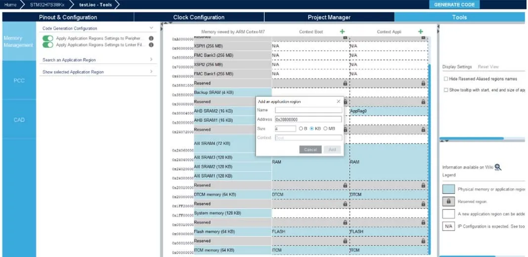
An example of MMT configuration of the OPENAMP Middleware on the STM32H755XIH6TR MCU 
Below are the steps for configuring the MMT with OPENAMP activated on the STM32H755XIH6TR MCU.
Choose a supported MCU.
Figure 463. Choose an STM32H7 dual-core product
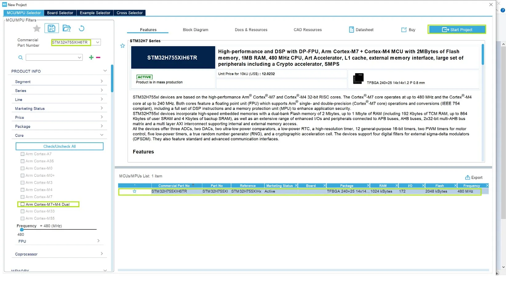
Click on the Start Project button, then choose Yes on the “Memory Protection Unit for Cortex-M7” dialog box.
Figure 464. Region 0 added
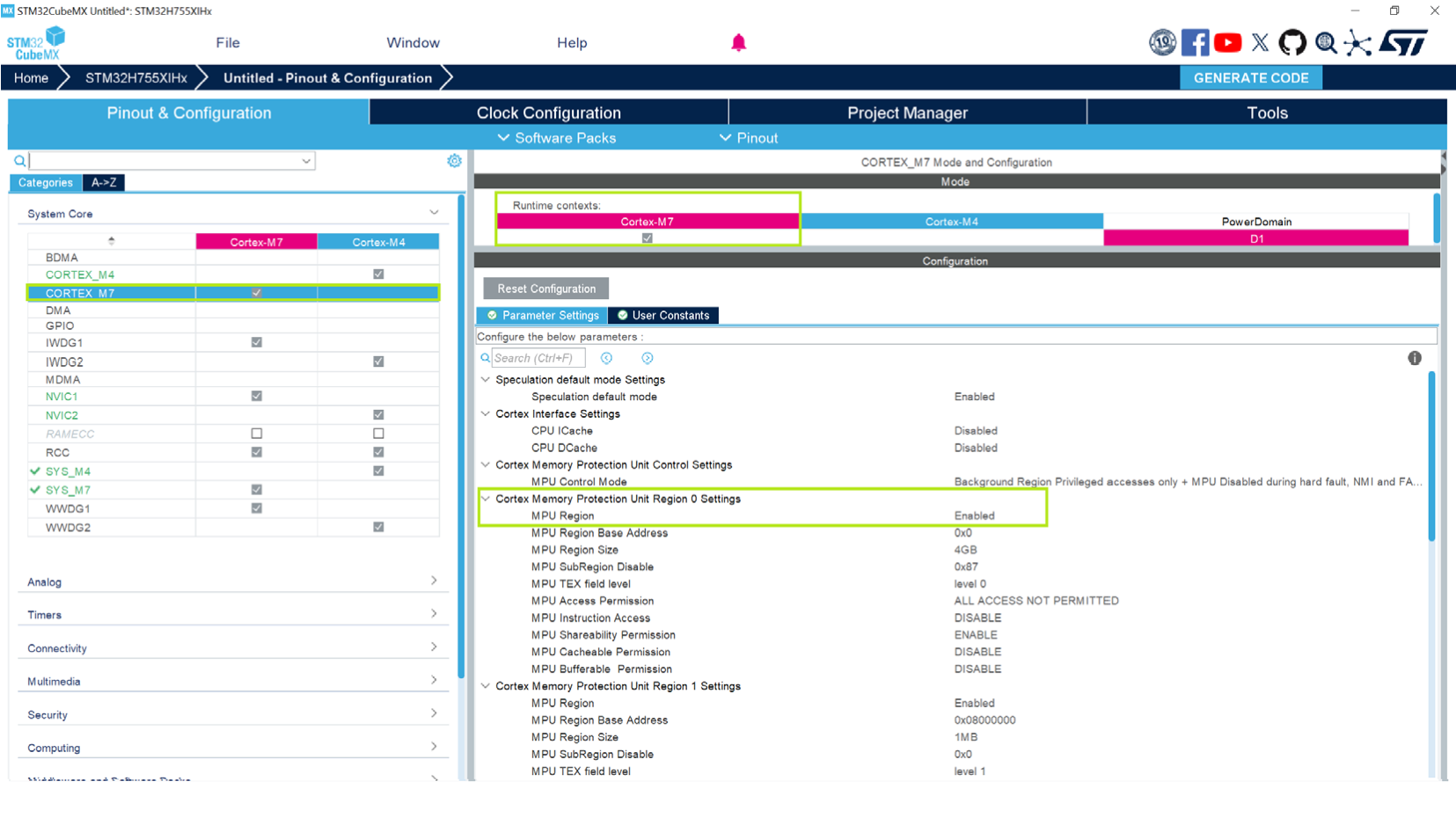
Note: STM32CubeMX applies the default configuration, then adds a 4 Gbytes region called “Region 0” under the Cortex_M7 parameters. The new parameters can be checked using the Pinout and Configuration tab.
Select “Tools” in the toolbar
Choose Memory Management.
Activate the Memory Management Tool support by clicking the button “Apply Application Regions Settings to Peripherals”.
Figure 465. Activate Memory Management support
Figure 466. Default setting for new application region

Add a new region by pressing the “+” button that appears in the white space when hovering with the mouse.
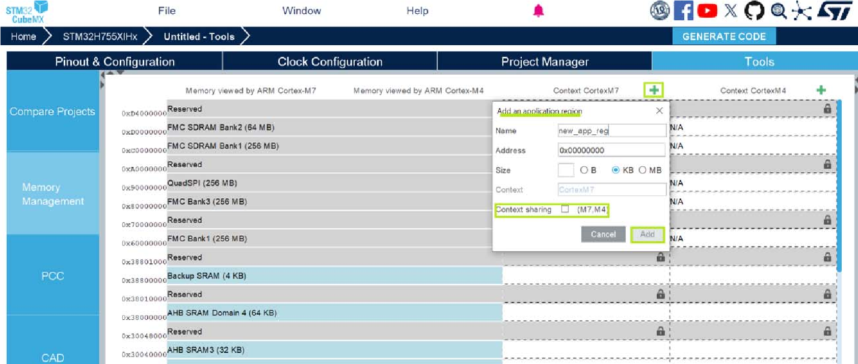
Select “Context sharing (M7, M4)”, automatically another region is created with the same name, start address, and size.

Select the Project Manager tab.
Give a name to the project and press the Generate Code button.
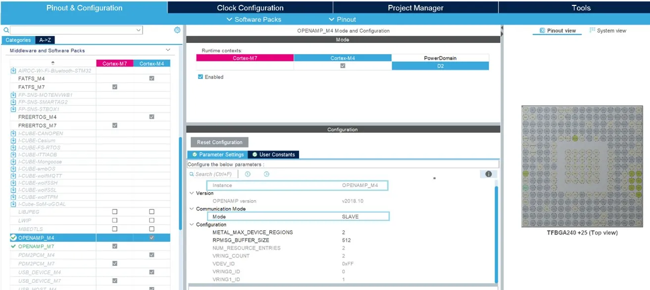
OPENAMP activation
Configure the NVIC1 and 2 and select their related HSEM global interrupts. – Activate the Middleware OPENAMP_M4.
MMT creates two application regions for each core. The Master regions are defined by attribute mode.
Figure 468. Configure NVIC1 and NVIC2, and select their HSEM global interrupt
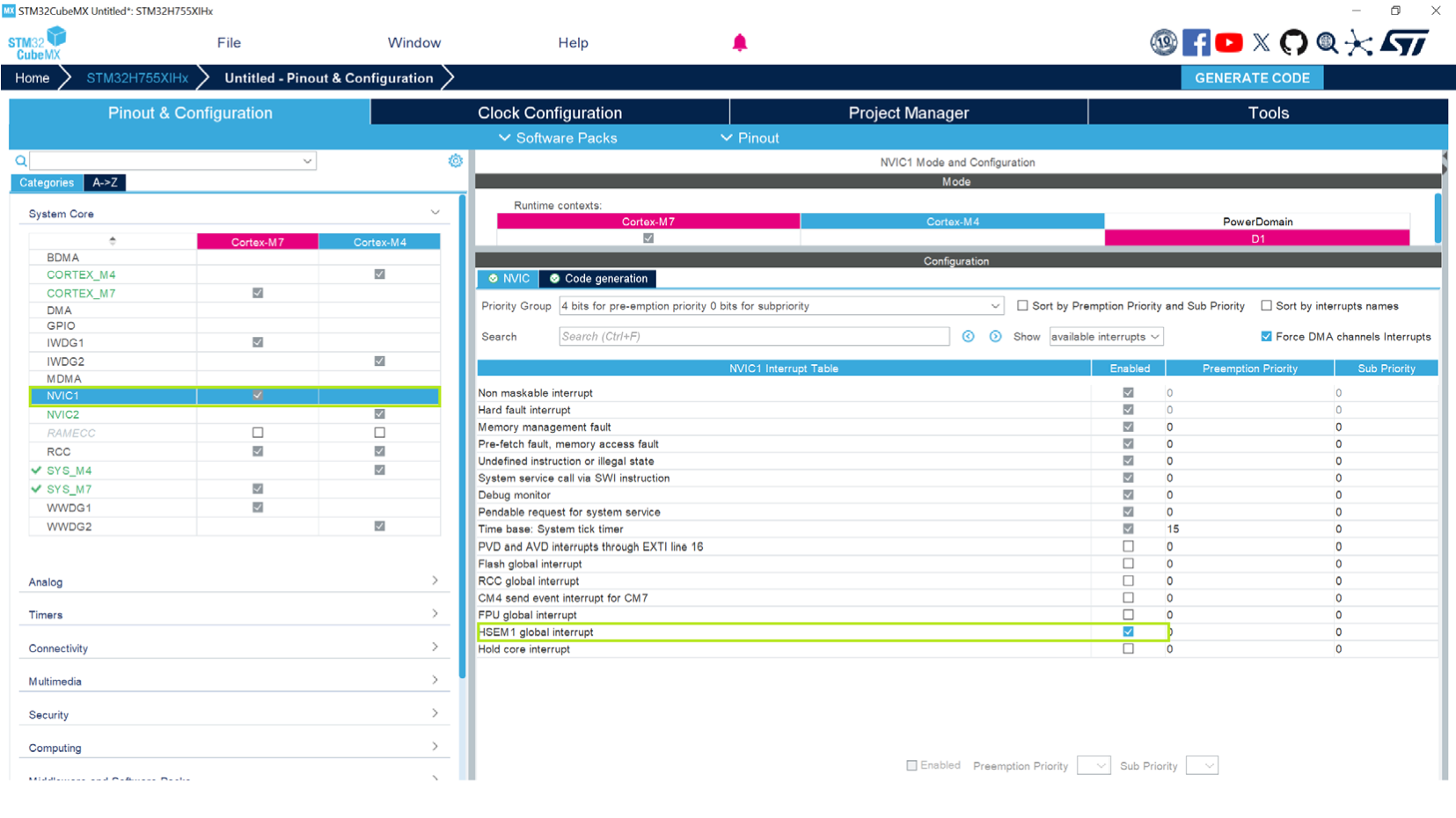
Figure 470. OPENAMP_M4 parameters settings
Press the Generate Code button to generate the code for both applications.
Apply Application Regions settings to linker files 
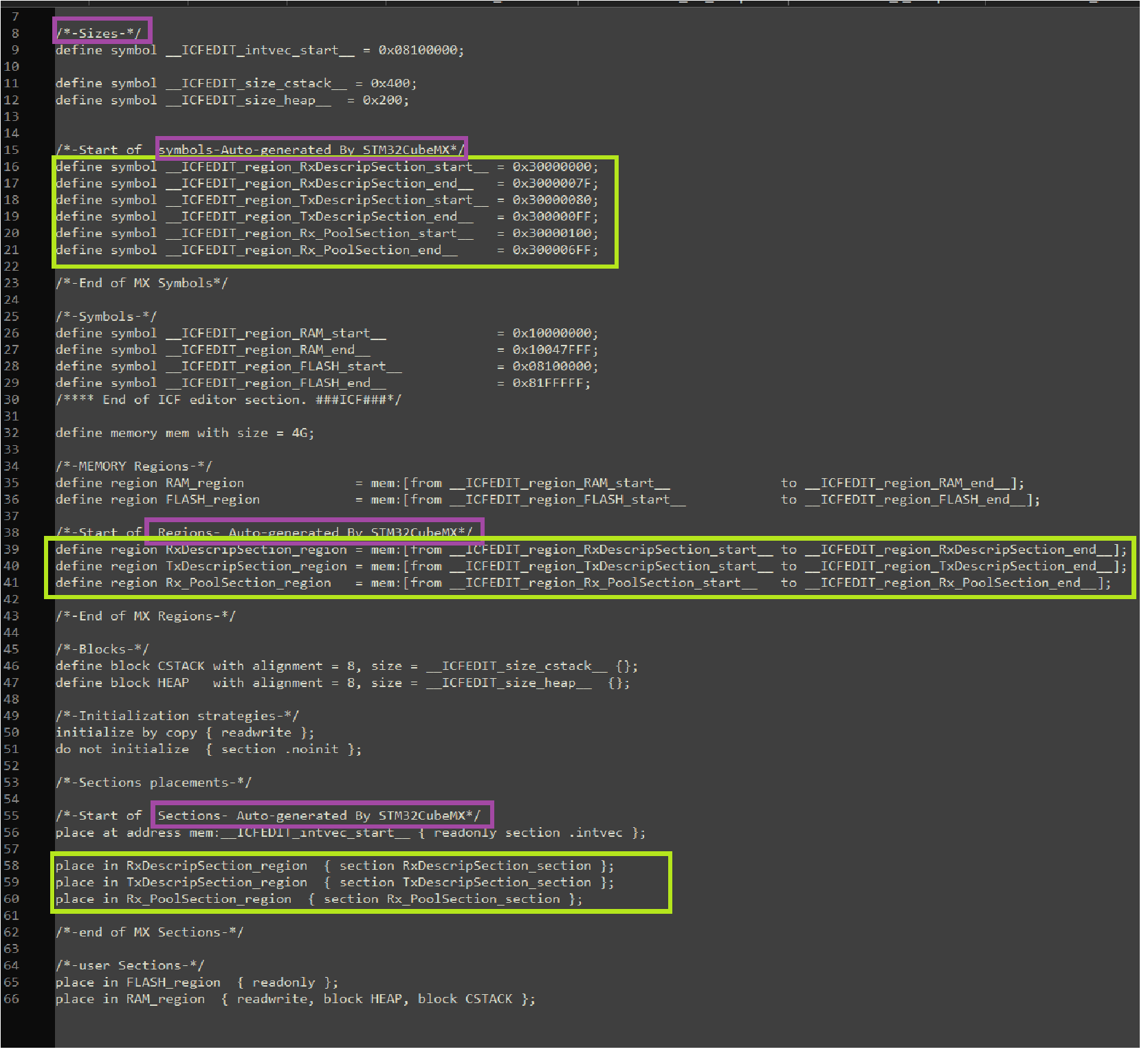
Figure 472. Linker files update (stm32h755xxx_flash_cm4.icf)
If disabled, it automatically chooses the configured memory along with the associated driver and sets the execution memory location in the linker file.
If enabled, the two regions and corresponding ‘export symbol’ must be added in the generated linker file.
After the code generation, navigate to the generated folder to check the linker file updates.
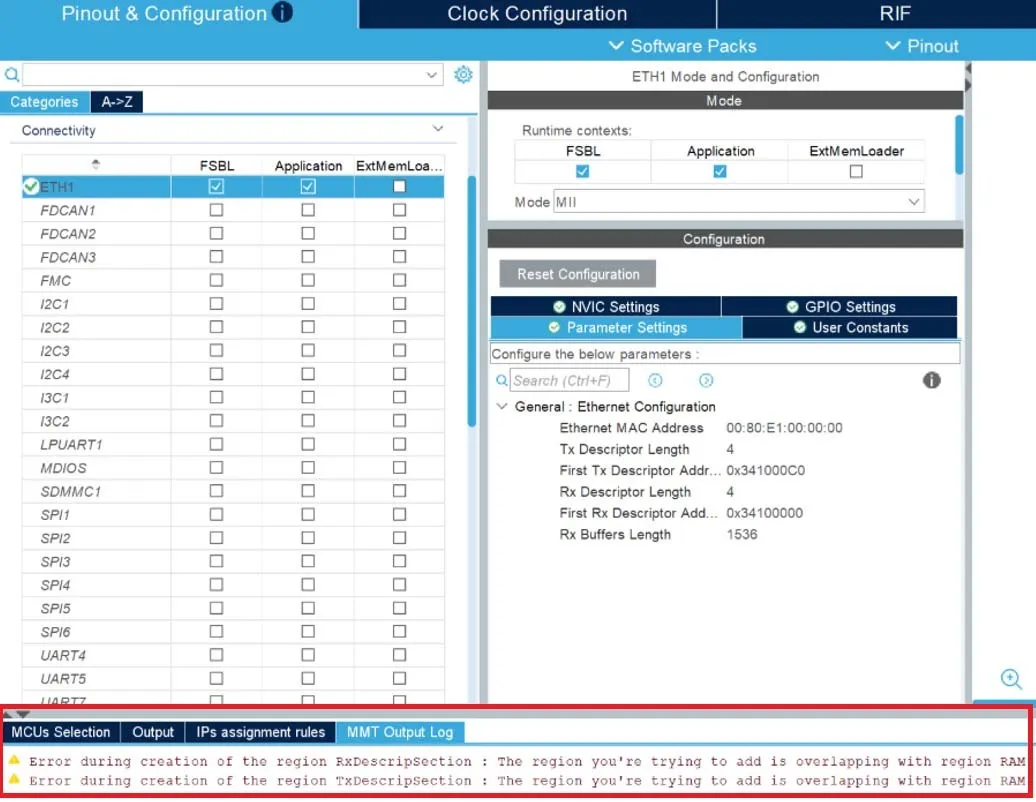
Example of MMT configuration of the ETH on STM32H755XIH6TR MCU 
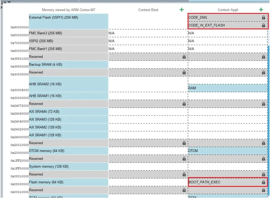
Activate the IP ETH: MMT creates three application regions for each core. To change the start address and the size of each region, update the ETH parameters.
Figure 474. Configuration of ETH IP

Press the radio button “Apply Application region Settings to Peripherals ON”, ETH will be partially under MMT control.
Press the Generate Code button to generate code for both applications.
Figure 476. IP configuration
When this button is on, the linker scripts for the CM7 project and CM4 project are generated, considering the configuration.
After the code generation, navigate to the generated folder:
Under the CM7 Project, open the linker definition file.
Under the Memories definition you can see the defined memories with their start address and length, according to the configuration made in STM32CubeMX.
Figure 477. Defined memories under the linker file (Cortex-M7)
Feature: MMT usage, pinout, and configuration user interface 
When the first toggle button is ON, Cortex-M7_BOOT (MPU) and Cortex-M7_APPLI (MPU) are under MMT control: their modes and parameters become read-only.

User interface 
Figure 480. Default settings
Region information 
Clicking on a particular region in the Application Regions column shows the associated details on the left hand side.
STM32CubeMX automatically adds a 4-Gbyte region for the system core, even if you are not planning to use the MMT.
Choose a supported MCU (the following example is based on STM32H7R3A8I6).
Figure 481. Choose an STM32H7R product
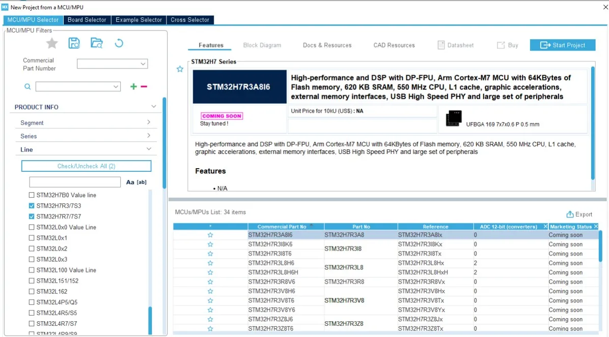
Click on the Start Project button, then choose “Yes” on the “Memory Protection Unit for Cortex-M7” dialog box.
Select the Tools tab:
Choose Memory Management
Activate the Memory Management Tool support by clicking on “Apply Application
Regions Settings to Peripherals”
Figure 484. Activate Memory Management support
Select the Project Manager tab
Give a name to the project and press the Generate Code button: a warning message is displayed.
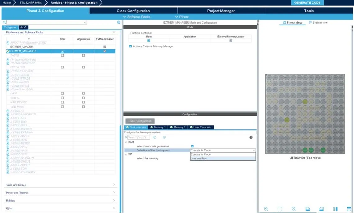
Select the Pinout and configuration tab
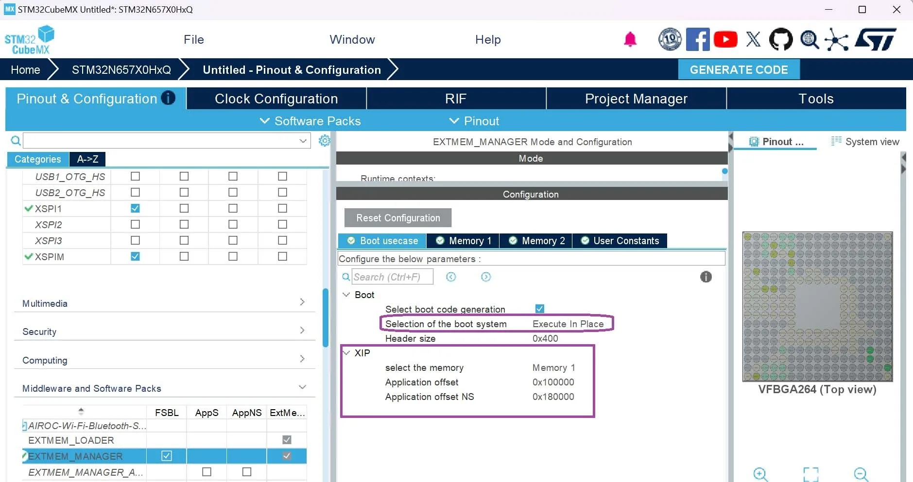
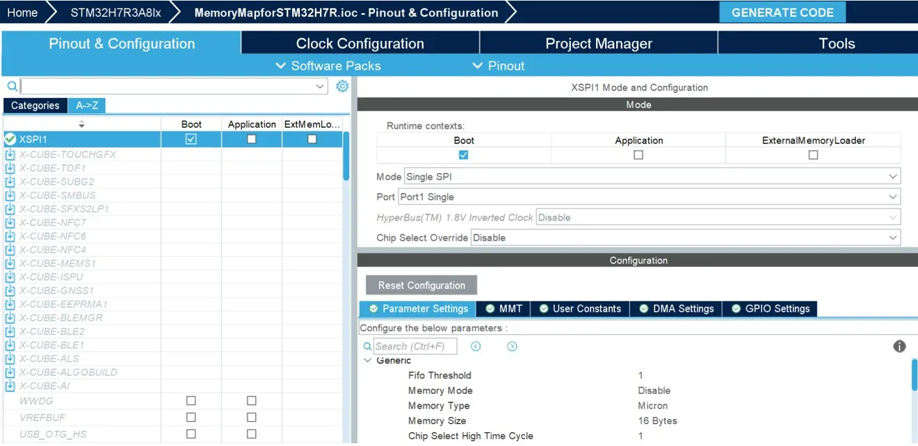
Enable XSPI1 for the boot context and choose the ‘Single SPI’ mode
Figure 486. Configure the XSPI
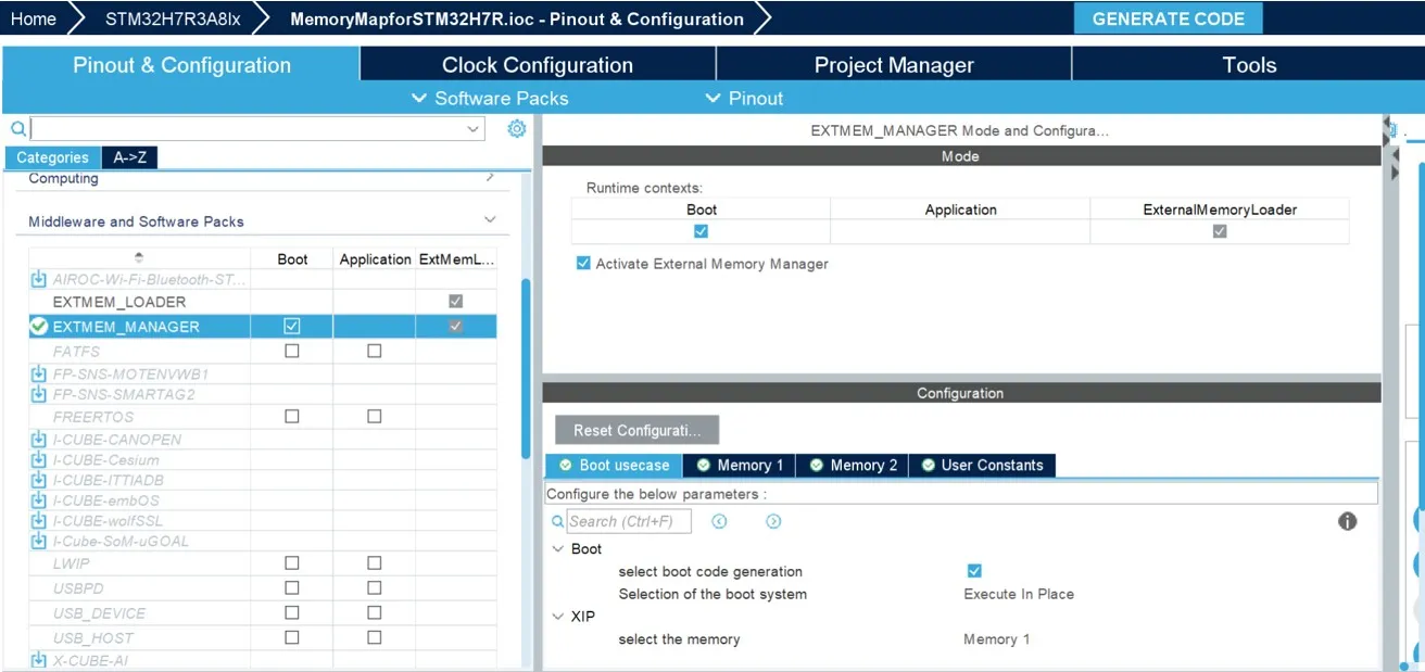
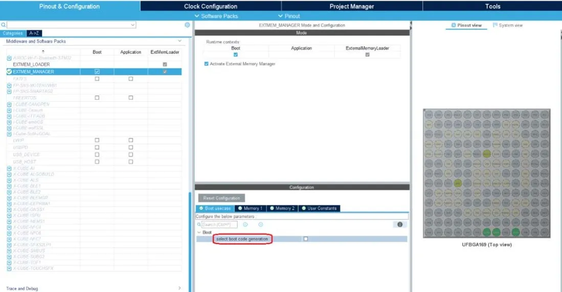
Activate the Middleware EXTMEM_MANAGER for the boot context:
> MMT solves the issue
> Press the Generate Code button to generate code for both applications. The overlap message does not appear any longer.
Figure 487. EXT_MEM_MANAGER
Code generation configuration 
The application regions settings can be applied to peripherals on the left-hand side of the screen. The concerned peripherals are shown on the associated tooltip. This can impact their availability on the pinout screen configuration.
Figure 488. Tooltip
Apply Application Regions settings to linker files 
When this button is on, the linker scripts for the Boot project and Appli project are generated, taking into account the configuration.
Figure 490. Linker files update
EXTMEM_MANAGER when using H7Rx/H7Sx 
The middleware can be used with the “Select boot code generation” disabled or enabled.
If disabled, MMT automatically chooses the configured memory along with the associated driver, and sets the execution memory location in the linker file. This is the most straightforward way of configuring an external memory.
If enabled, by activating the “Select boot code generation” you can choose “Execute in Place” or “Load and Run”
Execute in Place chooses and configures the memory zones
Load and Run lets the user choose source, destination memory, and addresses to jump to. The configuration is translated into the linker file. The user must provide the source and destination addresses.
Figure 492. EXTMEM_MANAGER “Select boot code generation” disabled
Under the boot Project, open the linker definition file. • Under the Memories definition you can see the defined memories with their start address and length, according to the configuration made in STM32CubeMX.
Figure 497. Linker files
ECC_ON_SRAM:
Linked to the AXI SRAM4 region on the MMT
When value is “disable” or “no update”, the AXI SRAM4 region size is set to 72 KB
When value is set to “enable” the AXI SRAM4 region is removed
DTCM_AXI_SHARED:
Linked to the AXI SRAM3 region on the MMT
When set to 0 or 3, the AXI SRAM3 region size is set to 128 KB, and the size of region named DTCM is set to 64 KB
When set to 1, the AXI SRAM3 region size is set to 64 KB, and the size of region named DTCM is set to 128 KB
When set to 2, the AXI SRAM3 region is removed, and the size of region named DTCM is set to 192 KB
ITCM_AXI_SHARED:
Linked to the AXI SRAM1 region on the MMT
When set to 0 or 3, the AXI SRAM1 region size is set to 128 KB
When set to 1, the AXI SRAM1 region size is set to 64 KB
When set to 2, the AXI SRAM1 region size is removed
Figure 499. ECC_ON_SRAM enabled and DTCM_AXI_SHARED set to 2
ETH impact on MMT when using H7RS/H7SX 
An example of MMT configuration of the ETH IP on the STM32H7R3A8Ix MCU
Activate the IP ETH:
MMT creates three application regions for each context.
To change the start address and the size of each region, update the ETH parameters.
Press the radio button “Apply Application region Settings to Peripherals ON”, ETH will be partially under MMT control.
Press the Generate Code button to generate code for both applications.
Apply Application Regions settings to linker files:
When this button is on, the linker scripts are generated, considering the configuration.
After the code generation, navigate to the generated folder:
Open the linker definition file.
Under the Memories definition you can see the memories with their start address and length, according to the configuration made in STM32CubeMX.
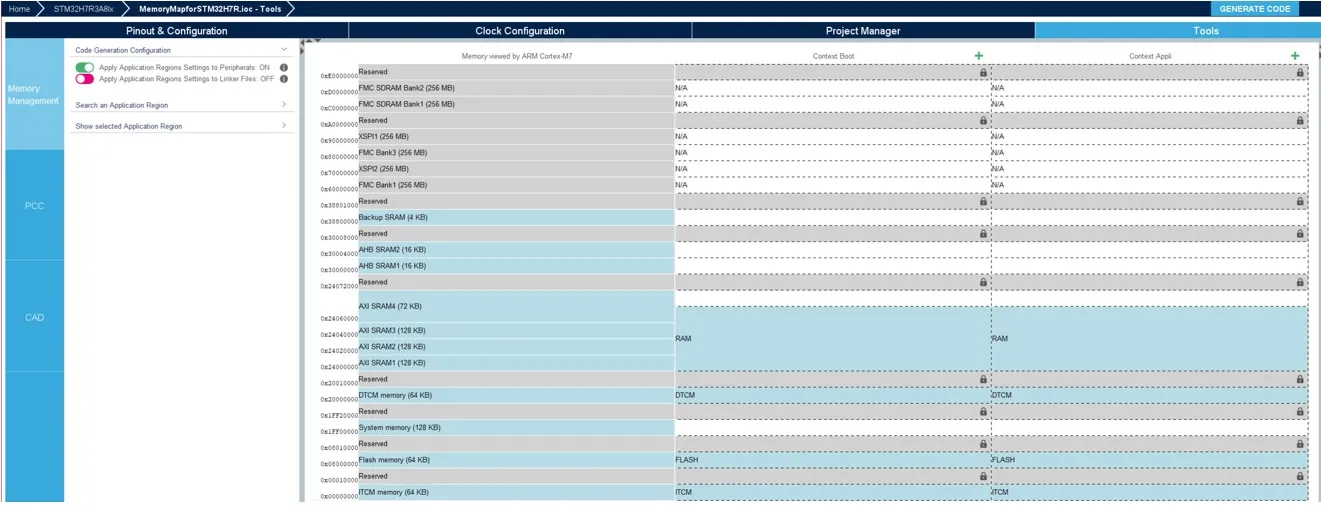
Figure 500. ETH MMT regions for STM32H7R3A8Ix
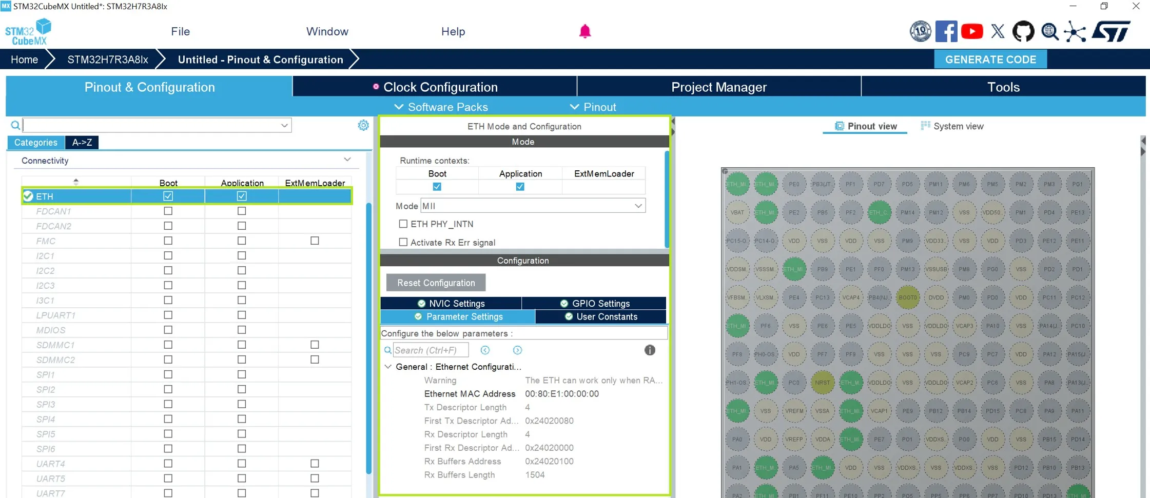
Figure 501. ETH configuration for STM32H7R3A8Ix
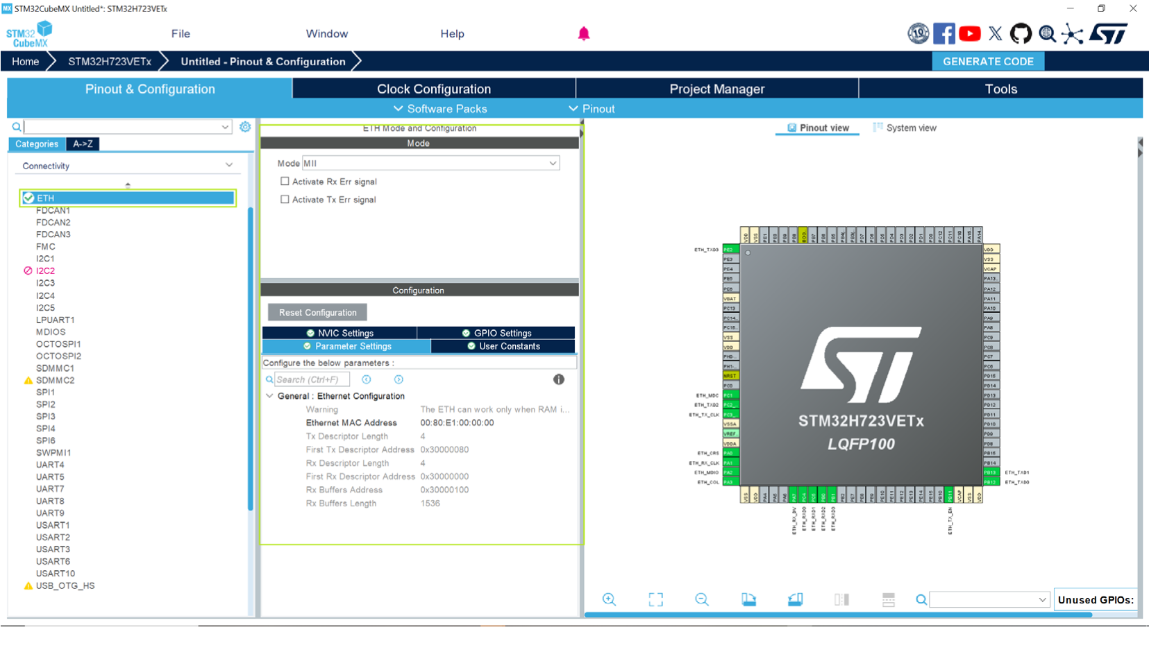
Figure 503. Defined memory regions under the linker file of the application context
Feature: MMT usage, pinout, and configuration user interface 
When the first toggle button is ON, Cortex-M0+ (MPU) is under MMT control: its modes and parameters become read-only (see Figure 504).
Apply Application Regions settings to linker files 
When this button is on, the linker scripts for the project are generated, considering the configuration.
The REGION_ROM is a default code region used in linker.
The linker file copies the STM32Cube firmware linkers files and only MMT region is updated or added.
OTA tag is not managed by MMT and usually exists in the linker file.
Figure 506. Linker files update
Impact on STM32WB09 RADIO 
When this IP is activated, a reserved region “Blue Core Config” calculated by value of CFG_NUM_RADIO_TASKS, which varies from 1 to 128, is added.
Figure 507. Impact on RADIO (STM32WB09)
MMT usage, pinout, and configuration of the user interface 
MMT interaction with peripherals starts from the moment the user enters their interfaces:
Checks their settings
Updates other peripherals involved in the memory map configuration
The peripherals are updated only when the first toggle button is “ON” in the panel Memory Management (under STM32CubeMx Tools).
Feature under MMT control for secure and nonsecure domains 
When the first toggle button is ON, the following features are controlled by MMT (their modes and parameters become read-only):
CORTEXM55-FSBL (MPU)
CORTEXM55_S (MPU)
CORTEXM55_NS (MPU)
SAU
RIF (RISAF panel)
Figure 508. Feature under MMT control (secure and nonsecure domains)
Feature under MMT control for secure domains 
When the first toggle button is ON the following features are controlled by MMT (their modes and parameters become read-only):
CORTEXM55-FSBL (MPU)
CORTEXM55_S (MPU)
RIF (RISAF panel)
Figure 509. Feature under MMT control (secure domains only)
Application regions for secure and nonsecure domains 
Only FSBL, CORTEX_M55_S, and CORTEX_M55_NS contexts are managed by the MMT. Each context has its own application region.
In the memory layout the CORTEX_M55_S and CORTEX_M55_NS use the same column for application regions.
Figure 510. Memory layout for secure and nonsecure domains
Application regions for secure domains 
Only FSBL and CORTEX_M55_S contexts are managed by the MMT. Each context has its own application region.
Figure 511. Memory layout for secure domains
Description of the memory layout in STM32CubeMX user interface 
The memory is split in three columns:
The left one is the memory seen by the core(s)
The middle one is the memory set-up for the application in FSBL context
The right one is the memory set-up for the application in the Context Appli
For the new project under STM32CubeMX, the tool creates the default application region to generate a valid project.
Region information 
Clicking on a particular region in the Application Regions column shows the associated details on the left-hand side.
Figure 512. Details about the clicked region in the FSBL context
Figure 513. Regions designation for secure and nonsecure domains
Example of using MMT with STM32N6 products 
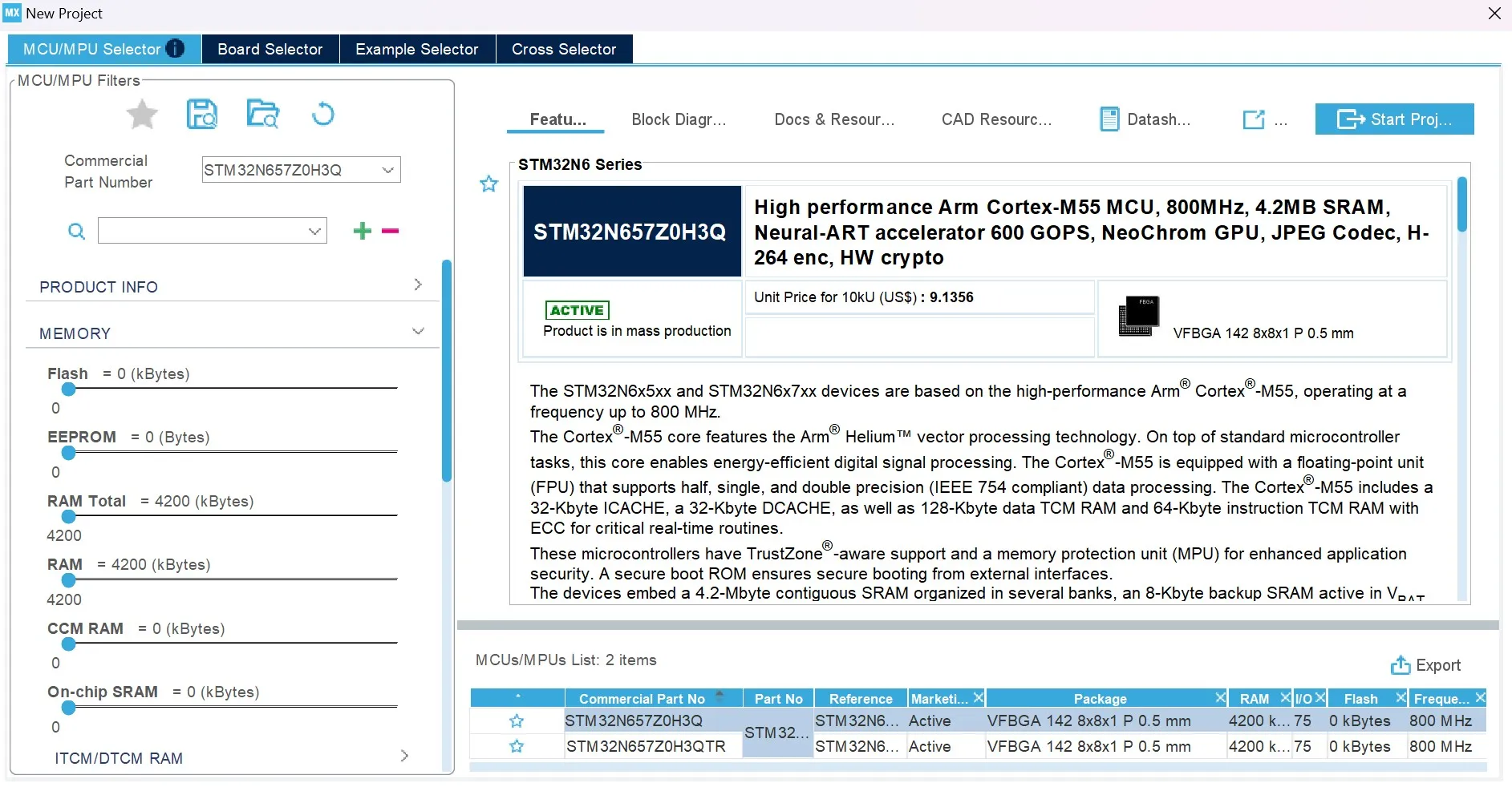
Choose an MCU that supports the MMT feature (the following example is based on STM32N657Z0HxQ).
Figure 515. Project creation with an STM32N6 product
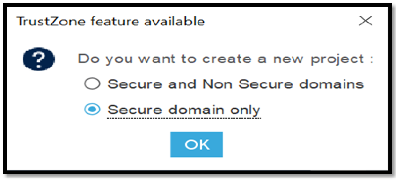
Choose the project structure, then initiate the project creation by clicking Start Project. Upon display of the TrustZone feature available dialog box, specify the domain configuration as Secure and Non-Secure domains before confirming with OK (Figure 516). Choose the second option if you intend to work exclusively within secure domains (Figure 517). STM32CubeMX applies the default configuration (RAM and FLASH regions are created in the MMT view).
Figure 516. Choosing the project structure (secure and nonsecure domains)
Configure the MMT
Click on the Tools tab
Choose Memory Management panel
Activate the Memory Management Tool support by clicking on “Apply Application
Regions Settings to Peripherals”
Figure 518. MMT configuration (secure and nonsecure domains)
Select the Project Manager tab
Give a name to the project and press the Generate Code button
Changes in RIF resulting from MMT activation 
By selecting “Apply Application region Settings to Peripherals ON,” the RISAF feature (located in RIF panel) is put partially under MMT.
The RAM and flash memory regions are configured with the same security, read/write, and privilege parameters. They are represented as a single RISAF region in the view corresponding to RISAF 2 (CPU AXI RAM0).
Figure 520. Mapping between MMT regions and RISAF memory configurations
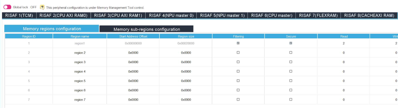
Configuration of memory regions in RISAF2 (CPU AXI RAM0) tab (region 2) 
Under the RISAF2 (CPU AXI RAM0) tab, region 2 has two groups of settings:
Fixed fields (grayed out): Region ID, Region Name, Start address Offset, Region size, and Filtering are read-only and cannot be modified.
Controllable fields (editable): The security and access parameters (Secure, Read, Write, and Privilege) are editable and are updated by the (MMT).
The values that MMT can set for the Read, Write, or Privilege fields are 2 (00000010b) and 0 (00000000b).
Figure 521. Setting up the memory region of RISAF2 (CPU AXI RAM0) tab
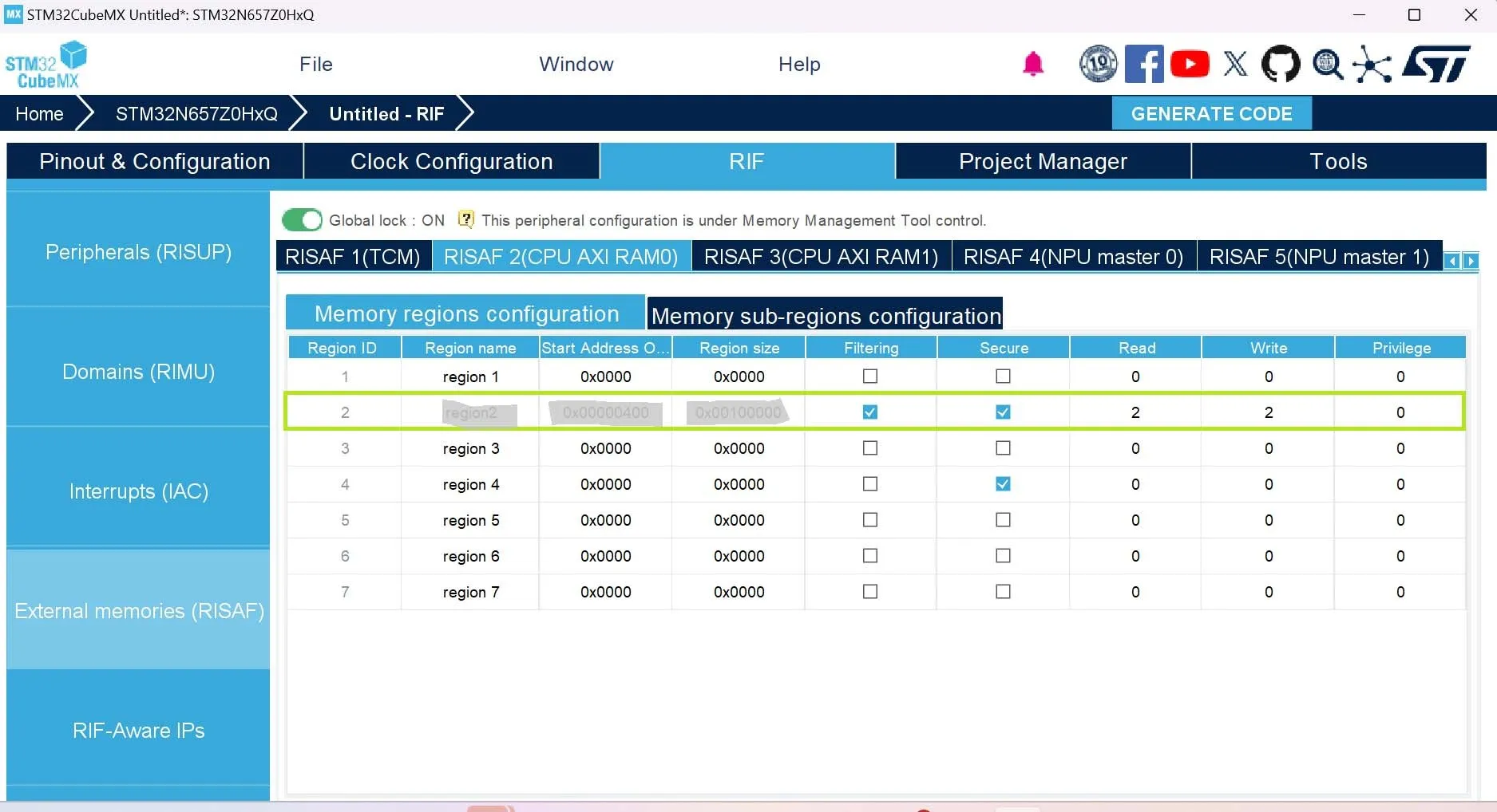
Setting up memory subregions for RISAF 2 (CPU AXI RAM0) region 2 
The Sub-Region A has two groups of settings:
Fixed fields (grayed out): RISAF Region ID, SubRegion name, Start address Offset, Region size, SubRegion CID (fixed to 1) are read-only and cannot be modified.
Controllable fields (editable): the security and access parameters (Secure, Read, Write, and Privilege are editable and are updated by the MMT.
Figure 522. Setting up memory subregions of RISAF 2 (CPU AXI RAM0) tab
Figure 523. Setting up memory regions of RISAF1 (TCM) tab
D-TCM is set to SYSCFG_DTCM_256K
I-TCM is set to SYSCFG_ITCM_256K
When adding a 256 KB application region that overlaps the ITCM and DTCM ranges:
The configuration of RISAF1 (TCM) remains consistent for its allocated portion.
Any memory belonging to that region above 0x340020000 is automatically redirected
(or split) and configured under RISAF7 (FLEXRAM). This segment starts at 0x340020000 and is treated as the beginning 0x00000000 offset of the RISAF7 region.
Figure 526. Setting up memory regions of RISAF1 (TCM) and RISAF7 (FLEXRAM) tabs
D-TCM to SYSCFG_DTCM_256K, I-TCM to SYSCFG_ITCM_64K, or
D-TCM: SYSCFG_DTCM_256K, I-TCM: SYSCFG_ITCM_128K, or
D-TCM: SYSCFG_DTCM_256K, I-TCM: SYSCFG_ITCM_256K
a warning appears, indicating that the flash memory region overlaps with the memory area reserved to FLEXRAM.
Figure 527. Overlap with FLEXRAM
Region 1: start address 0x34200000, size 1792 KB in FSBL (S) context
Region 2: start address 0x24200000, size 1792 KB in Appli NS context
Figure 528. Configurations of the application regions on the MMT view
Two RISAF regions in RISAF4 (secure region, nonsecure region), see Figure 529
Two RISAF regions in RISAF5 (secure region, nonsecure region), see Figure 530
Two RISAF regions in RISAF6 (CPU master), see Figure 531
Figure 529. Setting up memory regions of RISAF4 (NPU master 0)
When the IP CACHEAXI is enabled, MMT must remove the address range shown in the figures below.
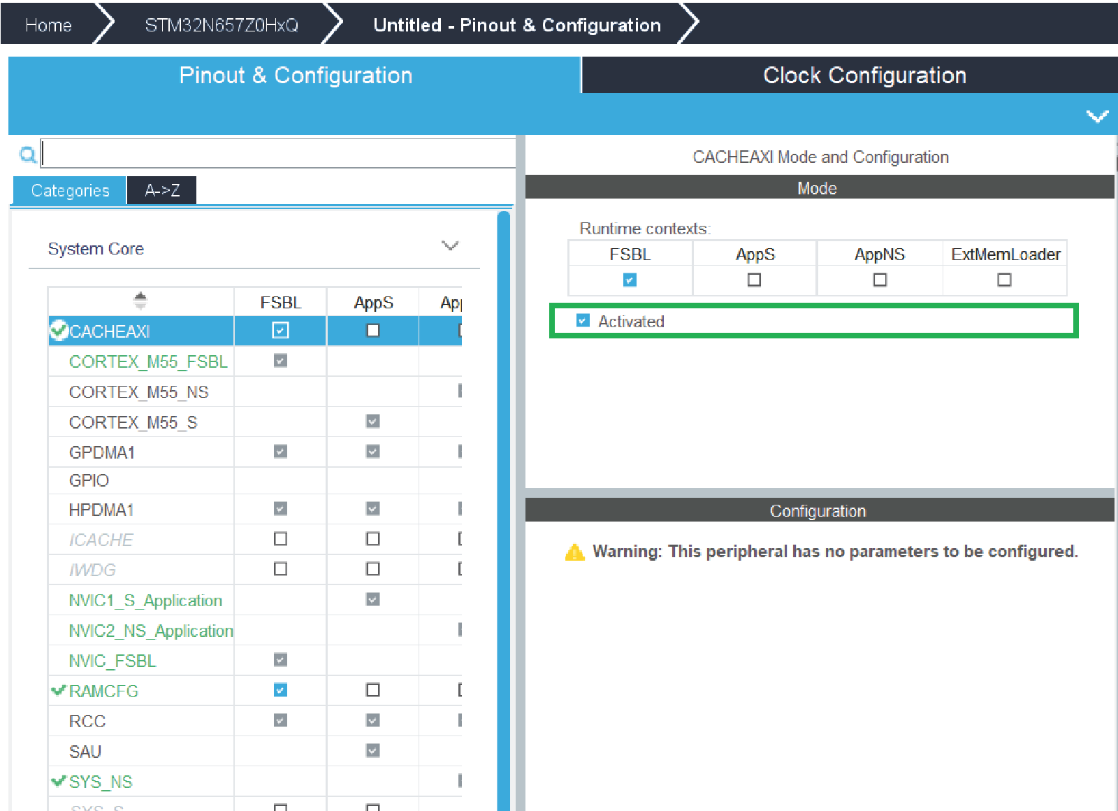
Add application region in CACHEAXI range (CACHEAXI must be disabled)
MMT add in RISAF 8(CACHEAXI) the regions with start offset like in MMT view RISAF9(VENCRAM):
When the IP VENC is enabled MMT must delete the range illustrated in the figure below.
Figure 536. VENC enable
Adding application region in VENCRAM range(user should disable VENC when it is activated)
Figure 538. Adding regions in VERCRAM
MMT add the regions in RISAF9 (VENCRAM) with start offset like in MMT view.
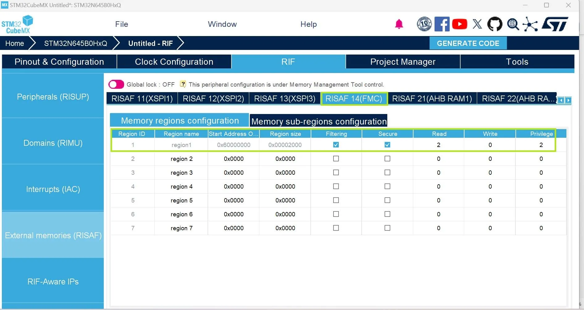
On RISAF14(FMC) tab the available FMC (Flexible Memory Controller) ranges include:
FMC Bank 1
FMC SDRAM Bank 1
FMC SDRAM Bank 2
Configuration:
Configure the FMC IP
Add application regions in FMC ranges
Figure 540. Configurations of FMC added regions in MMT view
EXTMEM_MANAGER 
Code generation configuration
The application regions settings can be applied to peripherals on the left-hand side of the screen. The concerned peripherals are shown on the associated tooltip.
The MMT configuration may impact their availability on the pinout screen configuration.
The EXTMEM_MANAGER can be used with the “Select boot code generation” parameter enabled or disabled.
If disabled, MMT automatically chooses the configured memory along with the associated driver and sets the execution memory location in the linker file. This is the most straightforward way of configuring an external memory.
If enabled, by activating the “Select boot code generation” you can choose “Execute in Place” or “Load and Run”
Figure 542. EXTMEM_MANAGER in the MMT view
Go to the Pinout and Configuration tab
Enable XSPI1 for the FSBL context and choose “Single SPI” mode
Activate the middleware EXTMEM_MANAGER in the FSBL context
Activate XSPIM and XSPI instances (XSPI1/2/3) Figure 543. Setting up the XSPI feature
Figure 544. Setting Select boot code generation parameter for EXTMEM_MANAGER
Execute In Place (Figure 545) chooses and configures the memory zones.
Load and Run (Figure 547) lets the user choose source, destination memory, and addresses to jump to.The configuration is translated into the linker file. The user must provide the source and destination address.
Figure 545. Selection of the boot system - Execute In Place
Figure 546. Configuration of the MMT view after enabling XIP
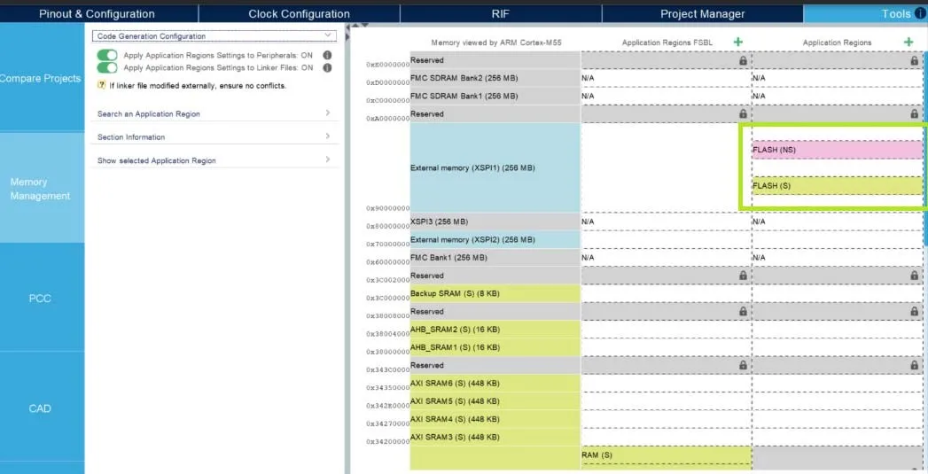
Figure 548. Configuration of MMT view after choosing Load and Run as boot system
Navigate to the generated project folder.
In the boot Project directory, open the linker definition file (usually an .ld or .icf file).
In the Memories definition section you can review the memory blocks (start addresses and lengths) that reflect your configuration settings.
Figure 549. Defined linker script for XIP
For secure domains:
Activate the ETH: MMT creates three application regions for each context Figure 551. ETH MMT regions for STM32N647L0HxQ
Update the start address and the size of each region, update the ETH parameters.
Press the radio button “Apply Application region Settings to Peripherals ON”, to make ETH partially under MMT control (Figure 552).
Press the Generate Code button to generate code for both applications.
Apply Application Regions settings to linker files:
Figure 552. MMT view after adding ETH memory regions
Open the linker definition file.
Figure 553. ETH linker file (fully secure domain only)
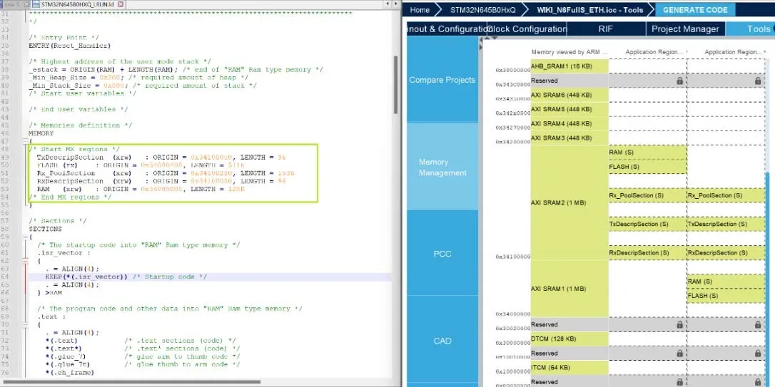
Figure 554. ETH MMT regions (secure domains only)
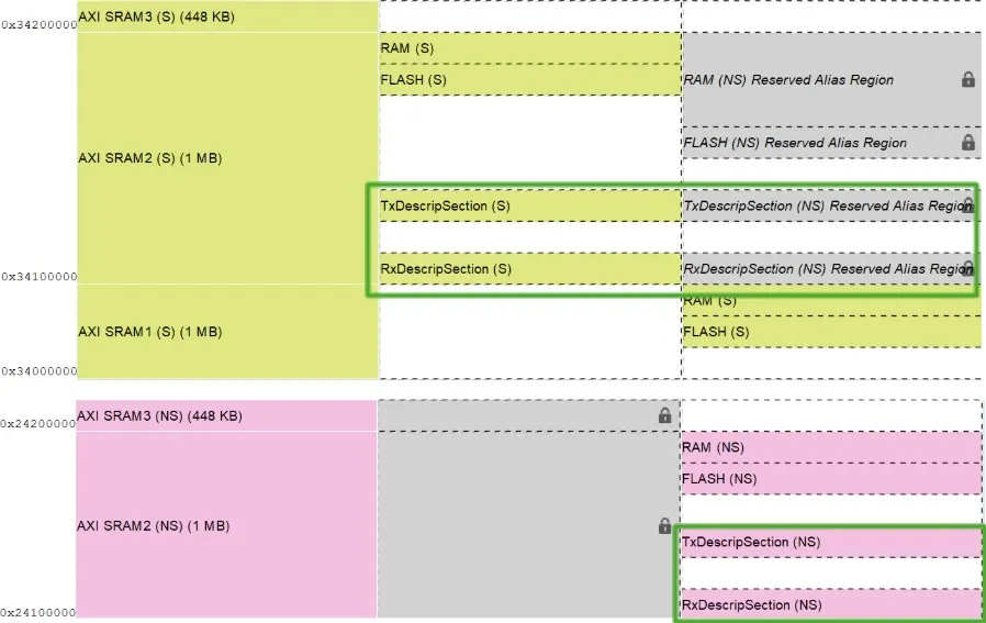
Under the Memory definition you can see the memory parts with their start address and length, according to the configuration made in STM32CubeMX. If an application region overlaps an ETH region a warning is displayed in the MMT log.
Figure 555. Warning in case of overlap between application and ETH regions
The default parameters are used for the secure context, but if the selected context is nonsecure, other nonsecure parameters are displayed.
Impact of configuring the ETH memory regions with ETH on RISAF panels 
Figure 556. RISAF 3 (CPU AXI RAM1) memory regions
5.5.9 Notification MMT/boot path (STM32H7RS and STM32H5) 
After the activation of boot path and MMT, all regions of MMT are deleted and replaced by the regions of Boot path in Appli context.
In this example, we use the boot path OEM-iRoT for STM32H7RS and for STM32H5.
Figure 559. MMT/boot path (STM32H7RS)
Open the linker files STM32H7S3I8KX_OEMiROT_Appli_app.ld or